A high voltage gain solid-state transformer for integration of renewable energy and AC sources
October 26, 2024
Abstract
This paper introduces a novel high-voltage gain topology for a solid-state transformer, integrating a DC-DC converter and dual active bridge converters. The proposed design features three DC links operating at different voltage levels. The first DC link connects to a single-switch high step-up DC-DC converter, while the second DC link interfaces with an AC source via a rectifier, allowing the use of both DC and AC inputs. A high-frequency transformer ensures galvanic isolation between the sources and the third DC link. The DC-DC converter employs coupled inductors and voltage multiplier cells, offering distinct advantages such as a high voltage gain, reduced voltage stress on semiconductors, and minimized current ripple. These features make the topology highly suitable for transferring power from renewable energy sources, such as photovoltaic panels, to a high-voltage DC link in microgrid or nanogrid applications. The novelty lies in the combination of multiple voltage levels, high-frequency isolation, and the ability to handle both DC and AC inputs efficiently. An experimental prototype, delivering 620 W with a 25 V DC input and 110 V AC input, is built, and the results validate the converter’s effectiveness.
Introduction
By harnessing solar power, solar photovoltaic (PV) system helps to reduce reliance on fossil fuels, mitigate climate change, and contribute to a cleaner and more sustainable energy combination1,2. The integration of PV systems into the electrical grid has gained significant momentum in recent years due to the growing emphasis on renewable energy sources3,4,5. As PV installations continue to expand, there is a need for efficient and reliable power conversion technologies to maximize the utilization of solar energy6,7. In this context, solid-state transformers (SSTs) offer promising solutions for PV system integration, enabling improved power quality, increased energy efficiency, and enhanced grid stability8. An SST for PV refers to the application of SST technology specifically tailored for photovoltaic power conversion and integration9,10. It serves as an interface between PV arrays and the grid, transforming and controlling the power generated by the solar panels to match the requirements of the grid or local loads11,12. Unlike traditional transformers, SSTs utilize advanced power electronic components and control algorithms to provide a range of functionalities and benefits for solar PV systems13. One of the key advantages of SSTs in solar PV applications is their ability to enhance power quality. SSTs can actively compensate for voltage fluctuations, harmonics, and other grid disturbances, ensuring stable and reliable power supply14,15,16. This capability is crucial for PV systems as they are subject to variations in solar irradiation and fluctuating power outputs17. By regulating voltage levels and compensating for power quality issues, SSTs enable solar PV systems to operate at maximum efficiency and minimize the impact on the grid18. Another significant advantage of SSTs in PV application is their ability to optimize energy utilization and increase overall system efficiency19,20,21. SSTs can employ advanced control algorithms to track the maximum power point of the PV panels, allowing for optimal energy extraction under varying solar conditions22. Additionally, SSTs can enable bidirectional power flow, facilitating grid interaction and energy storage integration, such as battery systems. This flexibility in power flow management contributes to higher energy conversion efficiency and improved system performance23. Moreover, SSTs for solar PV can enhance grid stability and enable the seamless integration of solar PV systems into existing distribution networks. By advanced control capabilities, SSTs can provide grid support functions such as reactive power compensation, voltage regulation, and fault detection24,25. These features help mitigate grid fluctuations caused by intermittent solar PV generation and ensure a smooth and reliable integration of solar PV source into the grid26. Furthermore, SSTs offer compact and lightweight designs, allowing for easier installation and reduced space requirements compared to traditional transformers27. This is particularly beneficial for PV installations where space constraints are often a concern. The compact size of SSTs also enables their integration within the PV system itself, reducing the need for additional external components and simplifying the overall system architecture28. In conclusion, SSTs for PV applications represent an innovative and efficient solution for integrating photovoltaic systems into the electrical grid. They provide enhanced power quality, increased energy efficiency, and improved grid stability29. As SST technology continues to advance, we can expect to see wider adoption of SSTs in PV installations, contributing to the continued growth and development of renewable energy30. Advanced semiconductor materials and power electronic components are used for.
building SST31. To regulate the flow of electric power, they use high-frequency switching devices such as insulated gate bipolar transistors (IGBTs) or silicon carbide (SiC) MOSFETs. In contrast to traditional transformers, which rely on magnetic cores and copper windings, SSTs employ power electronics to transform and regulate electrical energy32. The key advantages of SSTs are their superior control, flexibility, and efficiency as compared to traditional transformers. Following are a few highlights and advantages: Voltage Regulation: SSTs can actively regulate voltage levels, allowing for improved power flow management and optimization. This allows for more efficient use of renewable energy sources, such as solar and wind, whose output is frequently variable33. Improved Power Quality: SSTs may actively adjust for power quality concerns such as harmonics, voltage sags, and swells. SSTs may also offer reactive power assistance, which improves the stability of the grid and dependability. Smart Grid integration: Advanced communication and monitoring capabilities may also be added to SSTs. This facilitates real-time monitoring, fault detection, and grid management by allowing for smooth integration with smart grid systems34. Compact and Lightweight Design: SSTs have a lower footprint and weight than standard transformers, making them easier to install and move. This is especially useful in cities or for adapting existing electrical infrastructure35. Energy Efficiency: SSTs are more efficient than traditional transformers, particularly under fluctuating load situations. Their capacity to actively manage power flow and eliminate losses helps in reduction of total energy consumption36.
In this paper, utilizing DC-DC and dual active bridge converters, a novel high-voltage gain structure of an SST is presented. The proposed converter comprises three DC links with varying voltages. The first DC link is connected to a high voltage gain DC-DC converter, that offers benefits like high voltage gain, low peak voltage of diodes and power switch, and low input current ripple. This enables the reception of power from renewable energy sources like PV panels through a high voltage DC link. The second DC link is connected to an AC source through a rectifier, allowing for the utilization of both DC and AC sources. A HFT is employed to ensure galvanic isolation between the sources and the third DC link. The proposed topology is studied using analysis for operational modes, steady state behavior. Finally, an experimental prototype is built which is capable of delivering 620 W power to output load at a switching frequency of 50 kHz, and the experimental results are presented.
Analysis of the proposed SST
The proposed SST is depicted in Fig. 1. This converter includes two sections. The first section is DC-DC conversion, and the other section includes three dual active bridge (DAB) converters and a high frequency transformer (HFT). Also, the proposed converter has three DC links (DC link-1, DC link-2, and DC-link-3). The voltage of DC link-1 is obtained by boosting of a low voltage renewable energy source like PV panel. The voltage of DC link-2 is obtained by rectifying an AC voltage source. DC link-3 is used to provide the dc input voltage for an inverter which transfers energy to an AC load. The summation of output AC voltages of DAB converters is applied to the primary winding of the HFT. The DAB converter in the secondary side of the HFT can operate as a rectifier and obtain a DC voltage for DC link-3. Therefore, the are used for building SST15. To regulate the flow of electric power, they use high-frequency switching devices such as insulated gate bipolar transistors (IGBTs) or silicon carbide proposed SST provides two AC ports and one DC port, and, three DC link with different voltages. DC-DC conversion section includes one power switch (S), four diodes (D1, D2, D3, and D4), five capacitors (C1, C2, C3, C4, and C5), one input inductor (Lin), and one coupled inductor. The turns ratio of the coupled inductor is defined as n = n2/n1. Each DAB converter has four switches. Also, the turns ratio of the HFT is presented as N = N2/N1. The PWM pulses of the power switches (S, S1, S2, S3, S4, Q1, Q2, Q3, Q4, So1, So2, So3, and So4), and main waveforms are depicted in Fig. 2. Based on this figure, the proposed SST operates in three main modes, and two transient modes. Because transient modes don’t affect steady-state analysis, only main operational modes are described in the subsequent subsections.
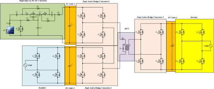
The proposed SST.
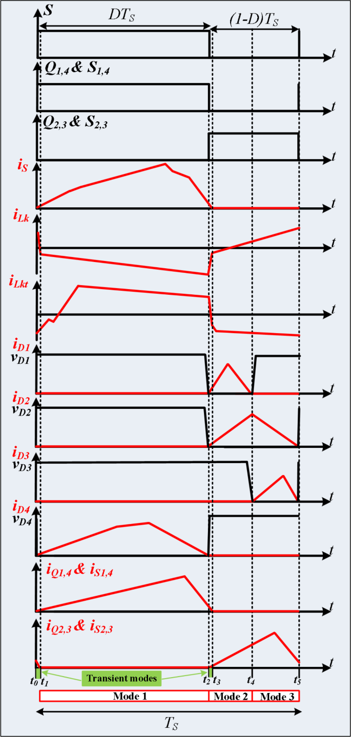
The main waveforms.
Operation modes
Mode 1 [t
0
< t < t
1
This mode starts when power switches S, S1, S4, Q1, and Q4 are tuned on. Power switches S2, S3, Q2, and Q3 are turned off during mode 1. Furthermore, the DAB converter in the secondary side of HFT operates as a rectifier and all switches of this DAB are turned off, and the current flows through anti-parallel diodes of switches So1~So4. The equivalent circuit of mode 1 is illustrated in Fig. 3 (a). As noted from this figure, the currents flowing through the switches S1, S4, Q1, and Q4 are equal. The voltage of DC link-3 is N(VDC1+VDC2). This mode ends at time instant, t = t1, when diode D4 is reverse biased.
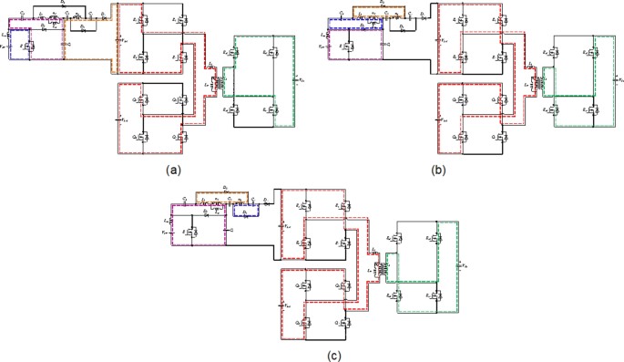
Operational modes, (a) mode 1, (b) mode 2, and (c) mode3.
Mode 2 [t
1
< t < t
2
At the start of mode 2, power switch S is turned off, and correspondingly, switches S2, S3, Q2, and Q3 are turned on. During this mode, Lin is discharged and its current is decreased. However, the voltage over Lm and Lk is positive and their currents are increasing. The standing voltages over switches S1 and S4 are equal to VC5=VDC1, and peak voltage across switches Q1 and Q4 are qual to VC=VDC2. The leakage energy of the coupled inductor is transferred to capacitor C3 through diode D2. Thus, the leakage energy is recycled during mode 2. The equivalent circuit of the converter during mode-2 is shown in Fig. 3 (b). Considering this figure, the following equations are obtained.
Mode 3 [t
2
< t < t
3
At time instant, t = t2, diode D1 is turned off and diode D3 is forward biased. The state of other semiconductor switches is same as that in mode 2. Since, the diode D4 is tuned off, therefore, the energy of solar PV source is not delivered to DC link-3. However, the stored energy of capacitor C5 is transferred to output capacitor Co through HFT windings. The configuration of this mode is depicted in Fig. 3 (c). During mode 3, the voltage across the capacitor C4 is as.
Voltage calculations
This section presents the calculation of voltage across the semiconductor switches, diodes and capacitors. Using volt-sec balance principle on input inductors, Lin and Lm, the expressions for VC1 and VC2 are obtained:
Substituting the value of Vc2 in (7), the expression for VC3 is
Also, substituting the value of Vc3 in (9), the expression for VC4 is
Substituting the values of Vc1, Vc2, Vc3 and Vc4 from (10), (11), (12) and (13) in (3), the simplified expression for Vc5
The voltage gain of DC-DC conversion section can be written as:
Furthermore, the ideal voltage gain is as follows:
The voltage of DC link-3 versus DC link-1 and DC link-2 can be expressed as:
The maximum blocking voltage over diodes D1, D2, and D3 can be calculated during mode 1, when these diodes are reverse biased. The expressions for Vd1, Vd2 and Vd3 are
Power switch, S and diode, D4 are turned off during mode 2. Thus, considering Fig. 3 (b), the maximum voltage across these elements can be obtained.
The normalized voltage stresses of semiconductors are presented by (24). Additionally, the variation of voltage gain, MDC/DC and voltage stresses across the switches and diodes versus coupled inductor turns ratio and duty cycle of power switch S are depicted in Fig. 4 (a) and (b). Plotting these figures, the voltage stresses across semiconductor switches and diodes in the DC-DC conversion section are normalized with respect to DC link-1 voltage (Vdc1=VC5).
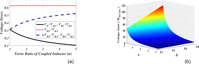
Voltage analysis, (a) normalized voltage stress (Eq. (24)) versus n and D = 0.6, and (b) The 3d view of the voltage gain MDC/DC.
Finally, the voltage stresses of power switches included in DAB converters are calculated as (25).
Current calculations
The average current of input inductor Lin can be obtained versus current of DC link-1:
The maximum value of current flowing through Lin is equal to algebraic sum of average current and half of peak-to-peak ripple:
The average currents flowing through the diodes in DC-DC conversion section are equal to Idc1. Based on the proposed SST’s configuration, the average current of power switch S is calculated as (28):
Therefore, considering the mean value, the peak current of switch S can be written as follows:
Considering the fact that, the average current of capacitors is zero, and using KCL, the average current of magnetizing inductance is obtained versus Is and ILin.
Also, the maximum current of Lm is
The peak current or current stress of diode D1 can be calculated during mode 2 operation, when the diode D1 is forward biased and is given by
The peak current of diodes D2, D3, and D4 are obtained as
Design of the components
This section presents the design consideration of the used components which are semiconductors, capacitors, and magnetic devices.
Semiconductors
The semiconductor switches and diodes of DC-DC conversion section and power switches included in DAB converters are selected based on maximum standing voltage and pathing current. These values are presented in the previous subsections of Sect. 2.
Capacitors sizing
The values of capacitors are calculated based on this assumption that; the ripple voltage is almost 2% of average voltage across the capacitor. Using the voltage and current in the pervious section, the minimum values of capacitors are attained as follows:
Inductors sizing
To achieve continuous conduction mode (CCM) of operation for DC-DC conversion section, which is suitable for renewable energy sources, the magnitude of ripples in inductor current is assumed to be lower than half of the average current. The minimum value of Lin and Lm is presented as (42) and (43).
The turns ratio of the coupled inductor (n = n2/n1) can be calculated based on Eq. (44):
High frequency transformer (HFT)
The HFT is selected based on the maximum voltage applied across the primary and secondary windings (VN1 and VN2), maximum pathing current of windings (IN1 and IN2), turns ratio (N = N2/N1), and switching frequency (fs) of the proposed SST.
Efficiency analysis
The efficiency of the proposed SST is analyzed using calculation of elements losses. The total loss is presented in (45), which includes loss of power switches, diodes, capacitors, and magnetic devices.
In (45), (Delta P)are the total loss, (Delta {P_S}), (Delta {P_D}), (Delta {P_C}), and (Delta {P_{Magnetics}}) power switches, diodes, capacitors, and magnetic devices losses.
Total Loss of power switches consists conduction and switching losses:
(P_{{Loss}}^{S}), (P_{{Loss}}^{{{S_{1 – 4}}}}), (P_{{Loss}}^{{{Q_{1 – 4}}}}), and (P_{{Loss}}^{{{S_{o1 – o4}}}}) are defined as (47):
In (47), ({r_{on}})is the on-state resistance, ts and tr are the falling and raising times of the power switches.
Total Loss of diodes includes conduction and forward voltage losses:
Where ({r_{{D_i}}})is the internal resistance during on state, ({V_{{F_i}}})is the forward voltage of didoes.
Furthermore, the total loss of capacitors and magnetic devices can be calculated using (49) and (50).
In (49) and (50), ({r_C}) and ({r_{{L_{in}}}}) are the ESR o capacitors and inductors. The average and peak values of currents flowing through the semiconductors included in DAB converters, current of capacitors in each mode, and RMS values of currents of all components, which are essential to calculate the power efficiency are listed in Table 1.
Experimental results
This section presents the experimental results of the proposed converter to verify the theoretical analysis. For this purpose, a prototype is built with 620 W output power. The parameters of the proposed converter are listed in Table 2. The presented topology can deliver power from two diverse power sources. One DC power source with voltage of 25 V is connected to the DC-DC converter. The coupled inductor turns ratio and duty cycle of power switch S is chosen as N = 1 and D = 0.6 to obtain an output voltage of 200 V at DC link-1. The DC-DC converter delivers a power of 200 W to DC link-1. Furthermore, an AC source with peak voltage of 110 V deliver 420 W to DC link-2 through a rectifier. After rectifying AC voltage, a 110 V DC voltage is obtained over DC link-2. Based on the configuration of the proposed converter, the summation of voltages of DC link-1 and 2, which is equal to VN1=200 + 110 = 310 V is applied to the primary winding of the HFT. The turns ratio of the HFT is 2:1. Thus, the voltage of secondary winding and also voltage of DC link-3 is equal to 155 V. The DC-DC converter includes 4 power diodes for which ultra-fast recovery STTH30R04 diode is used.
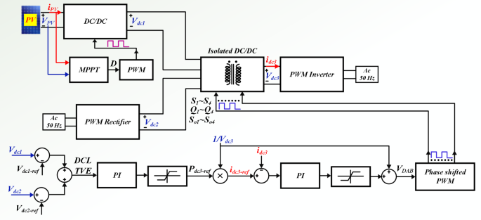
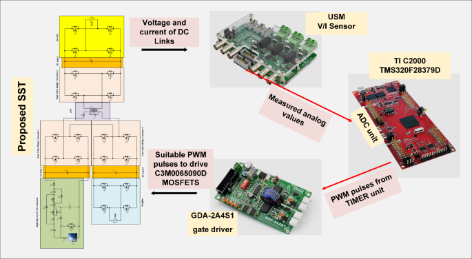
The power switch of DC-DC converter and power switches of the DAB converters are silicon carbide power MOSFET C3M0065090D. To generate PWM pules for power switches, TI C2000 TMS320F28379D launchpad is used. along with GDA-2A4S1 which is an isolated gate driver. Input value of inductance, Lin is selected to be 300 µH, while the magnetizing inductance, Lm of the coupled inductor is 300 µH, and its leakage inductance equal to 3 µH. To implement the input and coupled inductors, ferrite EE 55/28/21 cores are utilized. Also, all used capacitors are aluminum electrolytic, and the values of capacitances of capacitors C1 ~ C4 are330 µF each, while for capacitor C5 (DC Link-1) the selected value is 680 µF, capacitance of C (DC Link-2) is 1500 µF, and the capacitance value of output capacitor (DC Link-3), Co is 470 µF. Figure 5 (a) shows the voltage waveforms of the DC link-1, 2 and 3. The voltages of DC link-1, 2, and 3 are measured as 192 V, 108 V, and 150 V, respectively. The waveforms of voltages across the diodes D1 ~ D4 are depicted in Fig. 5 (b). Voltage of diodes D1, D3, and D4 is almost 60 V, and voltage of diode D2 is measured as 119 V. These values validate the relations given by (19)-(22). Between diodes, the maximum normalized standing voltage is related to diode D2, which is 119 V/192 V = 0.61. Figure 5 (c) depicts voltages of capacitors C1 ~ C4. Voltage across the capacitor C1 is measured to be 54 V, and voltage of capacitors C2, C3, and C4 are obtained as 36 V, 70 V, and 35 V, respectively. These results confirm the mathematical equations presented in (10)-(14). Figure 5 (d) illustrate the voltage waveforms of the coupled inductor’s primary winding, HFT secondary winding, and power switch S. The maximum voltage appearing across windings n1 and N2 of the HFT are measured as 37 V and 150 V. The peak voltage across the power switch S is obtained to be 58 V. Therefore, the normalized voltage stress of this switch is equal to 58 V/ 119 V = 0.48. The input current of the DC-DC converter and leakage inductance of the HFT are shown in Fig. 5 (e). The average value of the input current iLin is obtained 8.4 A, and peak to peak value of this current is 1.8 A. This experimental result validates that due to low value of ripples in input current, the DC port is suitable for renewable sources. Due to the AC from, the average value of the pathing current from HFT is almost zero. Also, the maximum pathing current form primary side of the HFT is measured 4.5 A, and peak to peak value of this current is 8.5 A. The measured efficiency versus output power is presented in Fig. 5 (f). The efficiency of the proposed SST for variation of output power from 50 W to 620 W is obtained between 91.55% and 94.1%. The maximum efficiency is measured at Po= 500 W, which is 94.1%. Also, at the rated power, the efficiency achieved is 93.81%. The DAB converters in the primary side of the HFT act like inverters. The PWM pulses of each leg in these inverters are complimentary with a dead band equal to 1 µs. The DAB converter in the secondary side of the HFT used as a rectifier. Therefore, it doesn’t need PWM pulses, and current paths though anti-parallel diode of power switches. The voltage across the power switches related to these three DAB converters are depicted in Fig. 6 (a)- (f). According to these figures, the maximum voltage across power switches S1 ~ S4 is equal to 192 V. Also, VQ1~VQ4 are measured to be 108 V, and VSo1~VSo4 are obtained as 150 V. Furthermore, considering Fig. 7, the effect of leakage inductance of the HFT is visible, which make spikes on the voltage waveforms of power switch S1 ~ S4, Q1 ~ Q4, and So1~So4. The experimental prototype is shown in Fig. 8. To measure the efficiency versus PV input, the ac voltage and output load (500 W) are considered constant. Then for different voltage values of DC source, the efficiency is measured. For this work, the dc voltage is set from 15 V to 25 V. For a constant value of output load, it is clear that, the power loss is reduced with increasing the input voltage. Therefore, with increasing input dc voltage, efficiency is increased, which can be seen in Fig. 7. The proposed control strategy is shown in Fig. 9. As can be seen, MPPT of PV can be obtained by DC-DC converter inside of the SST. In fact, one of the reasons of using high step-up DC-DC converter in the proposed SST is to track the MPP of renewable energy sources like PV panel. The voltage of DC link 1 and 2 (Vdc1 and Vdc2) are regulated by dual active bridge converters in the primary side of the HFT. To control of voltages of DC link 1 and 2, the DC links total voltage error (DCL TVE) is summed and DCL TVE is controlled by PI controller. The controlled signal is considered as the reference output power of dual active bridge in the secondary side of the HFT. Thus, the injected current to the PWM inverter can be controlled. Furthermore, the voltage of DC link-3 can be regulated by PWM inverter. Totally, the voltage regulation cannot be an unsolvable problem using a three stages SST. It should be noticed that, three stages SST has DC links in both primary and secondary sides of the HFT, and the proposed SST can be categorized as a three stages SST.
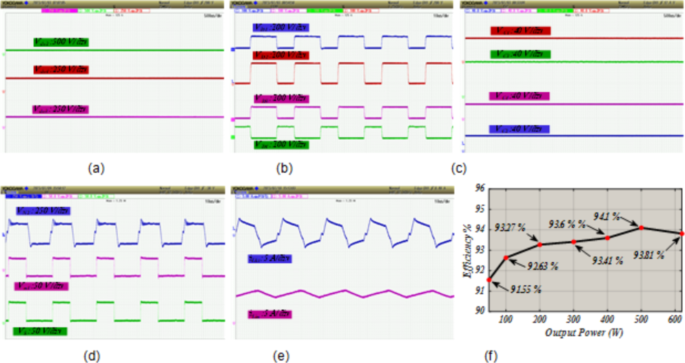
Experimental waveforms, (a) voltage of DC links, (b) voltage of diodes D1 ~ D4, (c), voltage of capacitors C1 ~ C4, (d) voltage of power switch S, primary winding of the coupled inductor and secondary winding of the HFT, and (e) current waveform of input inductor Lin and primary winding of the HFT, and (f) the measured efficiency versus Po.
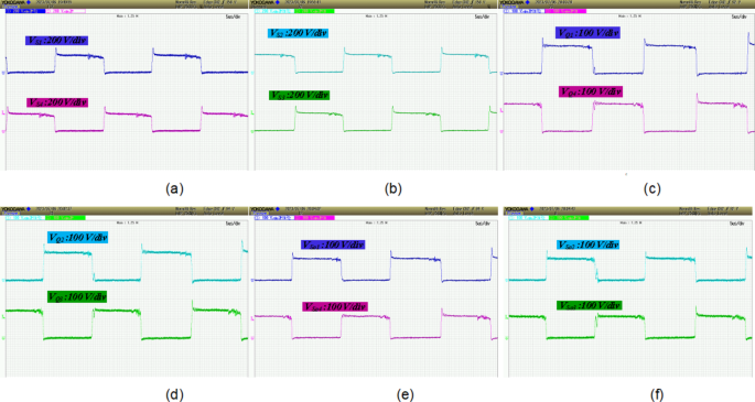
Experimental waveforms, (a) & (b) voltage of switches S1 ~ S4, (c) & (d) voltage of switches Q1 ~ Q4, (e) & (f) voltage of switches So1~So4.
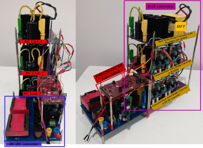
Experimental prototype.
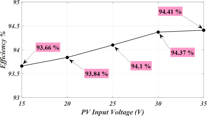
The efficiency curve versus PV input voltage.
The proposed control method.
Figure 10 illustrates the experimental control scheme for the solid-state transformer. In this scheme, the DC link voltages are regulated even when there are sudden changes in the PV and AC input sources. The corresponding experimental results are shown in Fig. 11, demonstrating the system’s performance under these varying input conditions. The proposed control method demonstrates the ability to effectively regulate the voltage of the DC links, even when there are fluctuations or variations in the input sources. This ensures stable performance and maintains the desired output despite changes in the input conditions, making the system more reliable and adaptable to dynamic operating environments. This capability is especially important for applications where input power may be inconsistent, such as in renewable energy systems, ensuring that the output remains steady and within the desired voltage range.
The experimental scheme for control of the proposed SST.
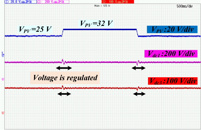
The closed-loop experimental waveforms.
Conclusion
In this article, a novel high-voltage gain topology of an SST is proposed. The converter presented consists of three DC links with different voltages. The first DC link is connected to a high voltage conversion ratio converter, offering advantages such as high voltage gain, low peak voltage of diodes and power switch, and low input current ripple. This allows power to be received from renewable energy sources like PV panels through a high voltage DC link. The second DC link is connected to an AC source via a rectifier, enabling the utilization of both DC and AC sources. Galvanic isolation between the sources and the third DC link is ensured through the use of an HFT. It should be noticed that, the third DC link is located in the output side of the converter. As a result, using HFT, the output port is isolated from input sources. The proposed topology is thoroughly surveyed by analysis of operational modes, steady state behavior, and efficiency Subsequently, an experimental prototype is built, capable of delivering 620 W of power to the output load at a switching frequency of 50 kHz, and the findings obtained from the experiments are showcased. The efficiency at rated power (Po=620 W) is 93.81%. Also, the maximum efficiency is obtained at Po= 500 W which is equal 94.10%.
Data availability
The data that support the findings of this study are available from the corresponding author upon reasonable request.
References
-
Chen, J., Zhang, Y., Liu, M., Chen, Y. & Zhu, R. Loadability Analysis of Smart Solid-State Transformer considering its interactions amongst all the ports. IEEE Open. Access. J. Power Energy, (2024).
-
Kopacz, R. et al. New single-stage bidirectional three‐phase ac‐dc solid‐state transformer. Electron. Lett. 60(2), e13084 (2024).
-
Li, Z., Hsieh, E., Li, Q. & Lee, F. C. High-frequency transformer design with medium-voltage insulation for resonant converter in solid-state transformer. IEEE Trans. Power Electron. 38(8), 9917–9932 (2023).
-
Li, Z., Zhao, C., Hsieh, Y. H., Li, Q. & Lee, F. C. Partial Fluctuation Power Control of Resonant Converter in Solid-State Transformer. IEEE Trans. Industr. Electron., (2024).
-
Mishra, D. K. et al. State–Space Modelling and Stability Analysis of Solid-State Transformers for Resilient Distribution Systems, Applied Sciences, vol. 14, no. 5, p. 2024. (1915).
-
Marzang, V. et al. A modified triple-switch triple-mode high step-up DC–DC converter. IEEE Trans. Industr. Electron. 69(8), 8015–8027 (2021).
-
Marzang, V. et al. A High Step-Up non-isolated DC-DC Converter with Flexible Voltage Gain. IEEE Trans. Power Electron., (2020).
-
Chaudhury, T. & Kastha, D. H5-CFDAB: a current-fed dual-active-bridge converter for application in modular DC Solid-State Transformer. IEEE Trans. Power Electron., (2023).
-
Wei, J., Feng, H. & Ran, L. Multidimensional Design of DC-Link for two-stage solid-state transformer cell considering second-order Harmonic current distribution. IEEE Trans. Power Electron. 38(8), 10244–10255 (2023).
-
Wei, T., Cervone, A. & Dujic, D. Active power decoupling for single-phase input-series-output-parallel solid-state transformers. IEEE Trans. Power Electron., (2024).
-
Hashemzadeh, S. M. et al. An ultra-high voltage gain interleaved converter based on three‐winding coupled inductor with reduced input current ripple for renewable energy applications. IET Renew. Power Gener. 18(1), 141–151 (2024).
-
Hashemzadeh, S. M., Hosseini, S. H., Babaei, E. & Sabahi, M. A soft switched high step-up DC‐DC converter based on VMC and coupled inductor for photovoltaic energy applications. IET Renew. Power Gener. 17(6), 1583–1596 (2023).
-
Zheng, L. et al. Solid-state transformer and hybrid transformer with integrated energy storage in active distribution grids: Technical and economic comparison, dispatch, and control. IEEE J. Emerg. Sel. Top. Power Electron. 10(4), 3771–3787 (2022).
-
Hashemzadeh, S. M., Babaei, E., Hosseini, S. H. & Sabahi, M. Design and analysis of a new coupled inductor-based Interleaved High Step-Up DC-DC Converter for renewable energy applications. Int. Trans. Electr. Energy Syst., vol. p. 7618242, (2022). 2022/09/09 2022.
-
Hashemzadeh, S. M. & Hejri, M. A fast and accurate global maximum power point tracking method for solar strings under partial shading conditions. J. Oper. Autom. Power Eng. 8(3), 245–256 (2020).
-
Hashemzadeh, S. M., Marzang, V., Pourjafar, S. & Hosseini, S. H. An Ultra High Step-Up Dual-Input single-output DC-DC Converter based on coupled Inductor. IEEE Trans. Industr. Electron., (2021).
-
Nayak, G. & Dasgupta, A. Series Inductance Estimation of Dual Active Bridge Converter in Solid State Transformer, in IEEE International Conference on Power Electronics, Drives and Energy Systems (PEDES), 2022, pp. 1–5: IEEE. (2022).
-
Valedsaravi, S., Aroudi, A. E. & Martínez-Salamero, L. Review of Solid-State Transformer Applications on Electric Vehicle DC Ultra-Fast Charging Station, Energies, vol. 15, no. 15, p. 5602, (2022).
-
Imanlou, A. et al. A New High Voltage Gain Transformer-less Step-Up DC-DC Converter with double Duty-Cycles: design and analysis. IEEE Access., (2024).
-
Nadermohammadi, A. et al. Cost-effective soft-switching ultra-high step-up DC–DC converter with high power density for DC microgrid application. Sci. Rep. 14(1), 20407 (2024).
-
Zarrinehbafan, M., Seifi, A., Nadermohammadi, A. & Hosseini, S. H. A new single magnetic core coupled-inductor based active switched quasi Z-source inverter. Sci. Rep. 14(1), 17197 (2024).
-
Zhang, J. et al. Control of a hybrid modular solid-state transformer for uninterrupted power supply under MVdc short-circuit fault. IEEE Trans. Industr. Electron. 70(1), 76–87 (2022).
-
Zheng, L., Kandula, R. P. & Divan, D. Predictive direct DC-Link control for 7.2 kV three-port low-inertia solid-state transformer with active power decoupling. IEEE Trans. Power Electron. 37(10), 11673–11685 (2022).
-
Bhawal, S., Patel, H., Hatua, K., Vasudevan, K. & Bhattacharya, S. Solid state transformer based on naturally cell Balanced Series Resonant Converter with cascaded H-Bridge cells switched at Grid frequency. IEEE Trans. Power Electron., (2023).
-
Lee, E. S., Park, J. H., Kim, M. Y. & Lee, J. S. High Efficiency Integrated Transformer Design in DAB converters for solid-state transformers. IEEE Trans. Veh. Technol. 71(7), 7147–7160 (2022).
-
Hannan, M. A. et al. State of the art of solid-state transformers: Advanced topologies, implementation issues, recent progress and improvements. Ieee Access. 8, 19113–19132 (2020).
-
Mishra, D. K. et al. A review on solid-state transformer: a breakthrough technology for future smart distribution grids. Int. J. Electr. Power Energy Syst. 133, 107255 (2021).
-
Shadfar, H., Pashakolaei, M. G. & Akbari Foroud, A. Solid-state transformers: an overview of the concept, topology, and its applications in the smart grid. Int. Trans. Electr. Energy Syst. 31(9), e12996 (2021).
-
Zand, M., Nasab, M. A., Sanjeevikumar, P., Maroti, P. K. & Holm-Nielsen, J. B. Energy management strategy for solid‐state transformer‐based solar charging station for electric vehicles in smart grids. IET Renew. Power Gener. 14(18), 3843–3852 (2020).
-
Zheng, L., Kandula, R. P. & Divan, D. Soft-switching solid-state transformer with reduced conduction loss. IEEE Trans. Power Electron. 36(5), 5236–5249 (2020).
-
Shamshuddin, M. A. et al. Solid state transformers: Concepts, classification, and control, Energies, vol. 13, no. 9, p. 2319, (2020).
-
Nair, A. C. & Fernandes, B. G. Solid-state transformer based fast charging station for various categories of electric vehicles with batteries of vastly different ratings. IEEE Trans. Industr. Electron. 68(11), 10400–10411 (2020).
-
Bravo, P. et al. Modular multilevel matrix converter as solid state transformer for medium and high voltage AC substations. IEEE Trans. Power Delivery. 37(6), 5033–5043 (2022).
-
Zheng, G., Chen, Y. & Kang, Y. A modular multilevel converter (MMC) based solid-state transformer (SST) topology with simplified energy conversion process and magnetic integration. IEEE Trans. Industr. Electron. 68(9), 7725–7735 (2020).
-
Xu, J. et al. FPGA-based submicrosecond-level real-time simulation of solid-state transformer with a switching frequency of 50 kHz. IEEE J. Emerg. Sel. Top. Power Electron. 9(4), 4212–4224 (2020).
-
Zhuang, Y. et al. A multiport DC solid-state transformer for MVDC integration interface of multiple distributed energy sources and DC loads in distribution network. IEEE Trans. Power Electron. 37(2), 2283–2296 (2021).
Acknowledgements
This publication was made possible by Qatar University Collaborative Research grant # [QUCP-CENG-2022-571] from the Qatar University. The statements made herein are solely the responsibility of the authors.
Author information
Authors and Affiliations
Contributions
A. Seyed Majid Hashemzadeh: Formal analysis, Software, Writing – original draft, Writing – review & editingB. Mohammed A. Al-Hitmi: Project administration, Supervision, VisualizationC. Shirazul Islam: Data curation, Investigation, SoftwareD. Atif Iqbal: Conceptualization, Supervision, Writing – review & editingE. Hadi Aghaei: Software, Validation, Visualization, Writing – original draft, Writing – review & editingF. Seyed Hossein Hosseini: Data curation, Visualization, Writing – review & editingG. Ebrahim Babaei : Validation, Writing – original draft, Writing – review & editing.
Corresponding author
Ethics declarations
Competing interests
The authors declare no competing interests.
Additional information
Publisher’s note
Springer Nature remains neutral with regard to jurisdictional claims in published maps and institutional affiliations.
Rights and permissions
Open Access This article is licensed under a Creative Commons Attribution 4.0 International License, which permits use, sharing, adaptation, distribution and reproduction in any medium or format, as long as you give appropriate credit to the original author(s) and the source, provide a link to the Creative Commons licence, and indicate if changes were made. The images or other third party material in this article are included in the article’s Creative Commons licence, unless indicated otherwise in a credit line to the material. If material is not included in the article’s Creative Commons licence and your intended use is not permitted by statutory regulation or exceeds the permitted use, you will need to obtain permission directly from the copyright holder. To view a copy of this licence, visit http://creativecommons.org/licenses/by/4.0/.
About this article
Cite this article
Hashemzadeh, S.M., Al-Hitmi, M.A., Islam, S. et al. A high voltage gain solid-state transformer for integration of renewable energy and AC sources.
Sci Rep 14, 25471 (2024). https://doi.org/10.1038/s41598-024-77326-5
-
Received: 08 August 2024
-
Accepted: 21 October 2024
-
Published: 26 October 2024
-
DOI: https://doi.org/10.1038/s41598-024-77326-5
Keywords
Search
RECENT PRESS RELEASES
Related Post


