A life cycle assessment approach to minimize environmental impact for sustainable printed sensors
March 29, 2025
Abstract
A printed hybrid sensor tag for applications in disposable healthcare and environmental monitoring optimized toward sustainability is presented. Following a systematic Life Cycle Assessment according to ISO 14040:2006 guidelines, the global warming potential associated with various substrate-, electrode-, and sensing materials, as well as manufacturing and end-of-life strategies, are evaluated. Results show that the utilization of bio-based polyethylene and copper inks can minimize the global warming potential most effectively by up to 39% from 42gCO2eq to 25.7gCO2eq per sensor tag. Among manufacturing methods, screen printing coupled with intense pulse light curing emerges as the most eco-efficient combination. Recycling is the most sustainable end-of-life option, although infrastructure challenges impede its full implementation. The silicon sensor chip needed for data communication has been identified as environmental hotspot. This study offers a comprehensive environmental evaluation of sustainable printed sensors and highlights critical challenges and opportunities for the electronics industry, particularly in relation to material selection, recycling strategies, and system-level considerations.
Introduction
Disposable biomedical sensing applications and point-of-care diagnostics hold immense potential for advancing global health by addressing critical demands, such as distributed diagnostics in regions with limited access to laboratory facilities1, supporting remote care for aging populations, and easing the pressure on overburdened healthcare systems. While these innovations offer invaluable benefits, the parallel challenge of electronics production and disposal intensifies the escalating issue of electronic waste2. The 2024 Global E-Waste Monitor published by the International Telecommunication Union and the United Nations Institute for Training and Research reports that electronic waste reached a staggering 96Â billion kg in 2022, and it is projected to grow to 120Â billion kg by 2030 if current trends continue3. The environmental impact of electronic waste is profound, affecting air, water, and soil quality, and contributing to climate change through the release of greenhouse gases (GHG) during improper disposal. With the rise of personalized sensor patches and wearables, an additional concern is that many of these devices will not be disposed of properly and end up in municipal waste or, even worse, in the environment. One example drastically showcasing this issue is the Great Pacific Garbage Patch, an accumulation of plastic between Hawaii and California, estimated to be twice the size of Texas4.
Apart from the disposal, the production of electronics significantly impacts the environment due to the intensive consumption of raw materials and energy. For instance, the extraction and processing of rare earth elements and metals required for electronic components contribute to habitat destruction, water pollution, and significant carbon emissions5. Furthermore, the environmental impact of electronics fabrication itself is significant due to its high energy consumption, notably in processes such as semiconductor fabrication and circuit board manufacturing. Additionally, the use of chemicals and generation of material waste during etching processes exacerbate environmental concerns. In the context of disposable medical wearables and point of care diagnostics, a trend towards eco-conscious development has emerged6,7. On one hand, a growing tendency in utilizing bio-sourced and recycled raw materials, such as paper8, paper-based9, and bio-polymeric substrates10, is observed. Biopolymer or bioplastic are general terms describing polymers that are biobased or biodegradable or both11. This means that bioplastic can be petroleum-based yet biodegradable, whereas bio-based plastic, despite being derived from renewable sources, is not necessarily biodegradable. There are several standards for defining “biodegradable,� and the criteria vary depending on the environment (e.g., soil or water)12,13. Generally, a certain percentage (e.g., ≥ 60%) of the material must degrade within a specified timeframe, typically between 3 and 24 months. Although it might seem intuitive that choosing biodegradable plastics would be a more environmentally friendly choice for substrate material, current literature remains divided on their potential to reduce pollution11,14. Due to the organic origin, biopolymers capture carbon dioxide from the atmosphere, leading to a reduced or even negative CO2 balance in their production15. When considering landfilling and composting, the perceived benefits of biodegradable plastics might diminish, as they often require specific conditions for degradation, such as elevated temperature and humidity. Some studies also suggest that while the degradation products of bioplastics are non-toxic, they might inadvertently affect soil acidity and microbial diversity11.
For manufacturing, additive technologies such as printed electronics are often presented as a more environmentally friendly alternative. This is due to the reduced number of processing steps, lower energy consumption as no cleanroom environment or high temperatures are employed, and less material wastage compared to traditional electronics production16. However, reliable data supporting the environmental benefits of printed electronics are sparse, typically focusing on RFID antennas, necessitating more evaluation through Life Cycle Assessment (LCA) approaches.
While most of a product’s environmental impact is generated during its production, use, and end-of-life (EoL) stages, the majority of this impact is determined during the design phase17. Moreover, sustainability considerations at the research stage are crucial in paving the way for the development of products with reduced environmental footprints. LCA is a systematic tool used to assess the environmental aspects and potential impacts associated with a product, process, or service by evaluating energy and material inputs and outputs at each stage of the life cycle. Originating in the 1960s and gaining prominence in the 1990s18, LCA has become an essential method in various industries, including automotive, civil engineering, agriculture, as well as electronics, to identify environmental hotspots and guide systematic sustainable decision-making. It provides a comprehensive view of environmental impacts, from raw material extraction through production, use, and disposal, enabling the comparison of different design and manufacturing strategies to minimize ecological footprints. A streamlined or comparative LCA is a simplified analysis focusing on key environmental impacts, often used to compare products or processes by assessing fewer indicators and focusing on the most relevant stages to reduce complexity.
The Global Warming Potential (GWP) is a fundamental measure used to evaluate the environmental footprint of products, providing insights into their role in climate change19. It quantifies the contribution of various GHGs to global warming by expressing their impact in terms of equivalent carbon dioxide (CO2eq) emissions over a specific timeframe.
The present work focuses on reducing the environmental impact of a printed hybrid sensor tag through LCA results. A systematic approach is used to identify environmental hotspots and compare design, manufacturing, and EoL options to determine the least impactful option in terms of global warming potential. The goal is to demonstrate a feasible pathway to sustainable point-of-care diagnostics and provide reliable data supporting the environmental benefits of printed and hybrid electronic systems. The sensor tag which is subject to this study is intended for wireless gas monitoring applications, such as health (e.g., breath analysis) or environmental monitoring. It builds on our previous work involving a Chitosan-based Acetone sensor integrated with a commercial passive near-field communication (NFC) sensor chip20.
Methods
The methodology of this study follows the ISO 14040:2006 standard21, which outlines the four key stages of Life Cycle Assessment (LCA): (1) Defining the objective and scope of the study, (2) Conducting an inventory analysis, (3) Performing an impact assessment, and (4) Interpretation of the results.
-
A.
Goal and Scope Definition.
The primary objective of this LCA is to optimize the design and manufacturing strategies for a printed wireless sensor tag designed for monitoring Acetone gas by identifying and quantifying the GWP, as illustrated in Fig. 1. The sensor tag is powered and read out through a commercial smartphone’s NFC function (Fig. 1b). This streamlined assessment aims to identify the most environmentally sustainable design choices among different materials and fabrication methods, ensuring that environmental considerations are integrated into the product development process. By focusing on the GWP, the aim is to assess the impact on climate change throughout the sensor tag’s life cycle. The functional unit for comparison is one sensor tag capable of wireless gas monitoring for an operational period of one day.
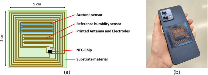
(a) Schematic representation of the sensor tag and its components; (b) use-case scenario of sensor tag attached to the case of a commercial smartphone.
The main components, as illustrated in Fig. 1a, and different design choices for the streamlined approach are listed in Table 1.
Figure 2d presents the model example of a sensor tag produced via inkjet printing of silver nanoparticles (NPs) onto a polylactic acid substrate. The conductive traces are cured using intense pulsed light, while the sensing layer consists of Chitosan. For EoL considerations, it is assumed that the sensor tag will undergo incineration with energy recovery. This sensor tag was developed with sustainability considerations in mind20 and serves as the reference configuration for the streamlined LCA.
The inventory of the substrates, inks, sensing materials, and manufacturing processes are summarized in Tables 2, 3 and 4, and Table 5, respectively. Based on that, the environmental impact is assessed. The configuration of the reference sensor tag is indicated with an asterisk. The ink demand for one functional unit varies with different printing technologies. While inkjet printing and Aerosol jet usually create traces with a layer thickness of around 2 μm, the typical thickness of screen-printed lines starts from 10 μm, depending on the type of mesh.
-
B.
Raw materials
Substrate materials
For the flexible substrate material, polylactic acid (PLA), petroleum-based polyethylene terephthalate (PET), bio-based PET (bio-PET), as well as bio-based polyethylene (bio-PE) are considered. Although Polyimide (Kapton®) is one of the most widely used plastic substrates in printed electronics and printed circuit boards22,23, there is no available LCA data on GHG emissions. Despite requests for information, suppliers did not provide details on its environmental impact; therefore, Polyimide is excluded from this study. PLA is a biopolymer and fabricated from renewable resources like corn through fermentation to produce lactic acid, which is then polymerized24,25. Under certain conditions, PLA can be considered as biodegradable11. PET, one of the most widely used plastics globally, is made from petroleum-based raw materials through esterification and polycondensation. PLA can be considered a substitute for PET due to its similar mechanical properties and other characteristics. Another alternative to PET is bio-PET 30, a bioplastic partially derived from renewable resources like sugarcane, which has gained increasing importance26. Terephthalic acid (TPA) and monoethylene glycol (MEG) are the monomer precursors which are then polymerized to produce PET. Currently, only the MEG component, accounting for 30% of the final polymer’s content, is available on a large scale from renewable materials, while the remaining 70% of commercial bio-PET 30 is still derived from fossil resources27. 100% Bio-PET, a fully bio-based alternative to conventional fossil-based PET, is not yet commercially available but has gained significant attention in scientific research due to its projected lower environmental impact and comparable mechanical properties. Companies like Coca-Cola28 and Toray Industries29 have recently showcased prototypes of 100% Bio-PET, demonstrating the material’s potential and the industry’s interest in bio-based alternatives. In contrast, bio-PE is commercially available in different versions up to 100% bio-based. It is mainly used as packaging material as well as for agricultural and horticultural films. It has lower mechanical and thermal stability compared to PET and just like bio-PET, bio-PE is not biologically degradable.
There are numerous other bio-based and biodegradable foils emerging in the market, but many of these materials have properties that limit their suitability for fabrication in printed electronics. For example, cellulose-based films, while appearing to be an attractive option due to their renewable origins and biodegradability, are commonly sensitive to moisture, which is incompatible with water-based inks and can compromise their mechanical integrity and performance in electronic applications.
Electrode materials
Silver (Ag) and Copper (Cu) are the most popular conductive electrode materials for printed electronics applications30.
Ag NP inks are favored for their excellent electrical conductivity and chemical stability, essential for high-performance electronic circuits. Cu inks are increasingly popular due to their lower cost compared to Ag and their good conductivity, which is suitable for many electronic applications. Cu’s affordability makes it an attractive option for large-area and disposable electronics. However, Cu inks are prone to oxidation and cracking during manufacturing, which can degrade performance and limit the durability of the devices.
NPs can be produced through manifold synthesis routines. Based on a study by Slotte & Zevenhoven31, an electrical arc method is assumed for NP manufacturing. While the process yield lies in the range of only 20%, which means that 5Â kg of raw materials is needed for the production of 1Â kg NPs, the surplus material is not wasted but can be recycled.
Carbon-based inks, largely used in some applications (e.g. biosensors32), have lower electrical conductivity compared to Ag and Cu30. This reduces the quality factor in printed antennas, where high conductivity is crucial for obtaining a stable connection for wireless sensor readout. Additionally, carbon-based materials are susceptible to cross-sensitivities to humidity and gases, which can influence their resistance33.
Similarly, magnesium (Mg), zinc (Zn), as well as conductive polymers, while offering biodegradable properties34, often face challenges in achieving the necessary conductivity for functional antenna structures or require additional treatments35,36.
Therefore, the study focuses on Ag and Cu as electrode materials.
Sensing materials
Chitosan: it is a natural and conductive biopolymer derived from chitin in crustacean shells, is a promising material for sustainable sensors due to its edibility, renewability, and environmental friendliness37,38. It is produced by treating chitin with an alkaline solution and offers a valuable use for waste materials from seafood processing. For the fabrication of the sensor, an aqueous Chitosan solution39, is drop-cast on the electrodes and dried at room-temperature forming a transparent film.
The electrical resistance of Chitosan is mainly influenced by the chemisorption of oxygen species on its surface. When a constant voltage is applied, electrons transition from the valence band to the conduction band, generating ionic species (O2−, O−) and decreasing the number of free electrons, which increases the resistance. However, when water is present, it facilitates the formation of O2 and the subsequent release of electrons, thereby lowering the sensor’s resistance. Acetone vapor in the air can disrupt the surface tension of the adsorbed water, making it easier for the water to evaporate. This occurs because the molecular vibrations of Acetone vapor agitate the water molecules, promoting more efficient evaporation. As a result, there is reduced interaction between water and oxygen species, which decreases conductance and causes the sensor’s resistance to rise and the capacitance to decrease with increasing Acetone concentration, as illustrated in Fig. 2a40. The Chitosan sensor exhibits a sensitivity that qualifies it for medical applications such as breath monitoring.
Zinc oxide (ZnO): ZnO is a semiconducting metal oxide that can be employed as sensing material for the detection of Acetone gas41. For the fabrication, an aqueous solution of ZnO NPs can be prepared and drop-cast onto the sensor electrodes followed by drying at room temperature. The sensing principle relies on the adsorption of Oxygen molecules onto the ZnO surface, where they become ionized into oxygen species by capturing electrons42. As humidity increases, sensor resistance decreases. When reducing gases like Acetone interact with these oxygen species, the trapped electrons are released back into the conduction band of ZnO. Consequently, the sensor resistance decreases while the capacitance increases with increasing Acetone concentration, as illustrated in Fig. 2b. This increase in capacitance can be explained by the release of electrons enhancing the charge carrier density, which allows the sensor to store more charge. At room temperature, the limit of detection of the ZnO sensor is roughly above 50 ppm. This qualifies it for applications such as industrial hygiene monitoring.
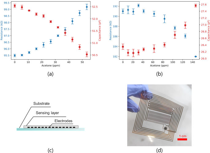
Capacitive and resistive sensor response of (a) Chitosan-based sensor: and (b) ZnO-based sensor to Acetone vapor – the error bars represent the standard deviation from the mean measurement values; (c) schematic representation of the sensor stack; (d) example of Acetone sensor tag with inkjet-printed silver electrodes and Chitosan sensing layer, as presented in20.
Sensor chip
The sensor tag is equipped with a commercial chronopotentiometric sensing chip (SIC4340, Silicon Craft, Thailand), which has a packaged size of 3 × 3 × 0.8 mm³. 2he chip is powered through energy harvesting from the electric field during readout, removing the need for a battery. In a single pass, the chip can efficiently read up to three different capacitive or resistive sensors.
-
C.
Manufacturing:

Manufacturing process flow of sensor tag including different options.
The manufacturing of the sensor tag consists of only four key steps which involve different options, as depicted in Fig. 3. First, the conductive antenna end electrodes are printed directly onto the substrate material using techniques such as inkjet printing (PixDro LP50, Suess MicroTech), screen printing (SCF300DE, Eickmeyer GmbH), or Aerosol Jet (Optomec) printing. Afterwards, the metallic layer is cured, which can be done either thermally in an oven or by means of intense pulse light (IPL) using a Pulse Forge (Novacentrix). For functionalization of the Acetone layer, the sensing materials are applied via drop casting directly onto the electrodes, as schematically illustrated in Fig. 2c. In the last step, the sensor chip is flip-chip bonded onto the tag using a micro-assembly station (Fineplacer, Finetech GmbH).
-
D.
System Boundaries:
The LCA encompasses the following stages:
-
Raw Material Extraction and Processing.
-
Manufacturing.
-
EoL Disposal.
These stages capture the key processes directly influenced by design and manufacturing decisions, thus affecting the GWP of the sensor tag, as illustrated in Fig. 4. The use phase and transport are excluded from this comparative LCA because there are no differences in these aspects due to varying material and manufacturing methods. Furthermore, during the operational phase of the sensor tag, no immediate environmental effects are expected as the printed device does not consume electrical energy directly, and any peripheral power supply (such as via radio waves) is excluded from this study.
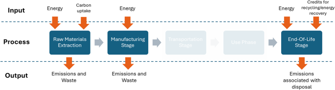
Schematic illustration of system boundaries, inputs and outputs of the LCA; The transportation and use phase are excluded.
The raw materials stage encompasses all GHG emissions associated with the resources and processes required for fabricating the virgin raw material, neglecting any contribution from recycling at this point. Instead, credits for recycling are attributed at the EoL stage. Final processing steps, such as converting plastic into substrate sheets, are excluded from this study due to the streamlined approach. Credits in the form of negative CO2eq are attributed to bio-based materials at this stage, reflecting the carbon uptake during the growth of plants.
In the manufacturing stage of this LCA study, the focus is on quantifying the GHG emissions associated with the electrical energy demand for fabricating the sensor tag. This includes energy requirements for all printing, curing, and chip integration processes essential to sensor tag production. Therefore, the duration of printing and curing per tag is estimated, varying across different processes. The study uses the GHG emissions associated with the European Union’s electrical energy mix in 2022 equaling to 0.251 kg CO2eq/kWh43, excluding emissions associated with general facility operations like building heating and cooling, or cleaning of tools, aligning with our streamlined approach focused on direct manufacturing process impacts.
EoL options refer to the various ways a product can be managed at the end of its useful life. The European Union (EU) waste framework directive from 200844 describes a hierarchy that outlines a strategy for waste management, prioritizing prevention, reuse, recycling, and energy recovery over disposal (e.g. landfilling, incineration). The emergence of novel technologies like wearables and point-of-care diagnostics poses challenges to conventional waste management. Personalized health and point-of-care diagnostic devices, due to their direct contact with the human body, are unsuitable for reuse because of hygiene considerations. Additionally, electrochemical sensors often have short lifespans and low stability levels, further reducing their reuse potential45. It can be assumed that a sensor tag used in personalized health will end up in municipal waste instead of being disposed of as electronic waste. In the EU in 2020, over half (59.1%) of the municipal waste underwent recovery processes: 39.9% was recycled, 12.7% was backfilled, and 6.5% was used for energy recovery. The other 40.9% of the waste was either sent to landfills (32.2%), incinerated without energy recovery (0.5%), or managed through other disposal methods (8.2%)46. Based on those considerations, three possible and practical EoL options were identified for the wireless gas sensor tag: (i) Landfilling; (ii) Incineration with energy recovery; and (iii) Recycling.
-
(i)
Landfilling: The sensor tag is entirely disposed of in a landfill which can be considered as a very likely scenario. Landfilling of carbon-based materials and in particular plastics contributes to GHG emissions primarily through the decomposition of organic components and the management of landfill gas. In this scenario, depending on the environmental parameters, biodegradable components of the sensor tag might degrade and release GHG emissions which are added to the EoL. However, non-degradable materials do not release significant amounts of GHG, which might give a misleading impression in terms of environmental impact. For instance, plastics in landfills can leach harmful chemicals and persistent organic pollutants into soil and groundwater, which is not reflected by GHG metrics. Degradation of plastics in landfills can lead to the generation of microplastics, which pose additional ecological risks47. Besides that, these materials persist for centuries, profoundly impacting aquatic life, wildlife, and ecosystems. This leads to eutrophication, contamination of groundwater and other long-term environmental impacts commonly classify landfilling as the least predictable and hence worst of all EoL options44.
-
(ii)
Incineration with energy recovery: The sensor tag is burned to generate energy. In this scenario, some of the CO2 emission is refunded at the EoL stage, as energy in the form of heat or electricity is recovered. The net impact ((:NI)) of the incineration process is calculated as48.
Where (:IE) is the incineration emission from burning the material. In this study this corresponds to the CO2 uptake of the material. (:AE) refers to the avoided emissions as the energy recovered from incineration displaces energy that would have come from fossil fuels. To calculate the avoided emissions for energy recovery in incineration, the following relationship applies49
(:NCV) is the net calorific value of the waste (in MJ/kg or kWh/kg), (:E_intensity) is the emissions intensity of the used energy mix (in kg CO2eq/MJ or g CO2eq/kWh), and (:eta_recovery:) is the energy recovery efficiency. In Europe, (:E_intensity=:0.251:kg:CO2:eq/kWh::) and (:eta_recovery:=0.25)50. In this study, the global warming potential is assessed for municipal waste incineration.
If no experimental data is available for NCV of a specific material, it can be calculated using Dulong’s Formula51:
where mC, mH, mO, mN, and mS represent the mass fraction of carbon, hydrogen, oxygen, nitrogen, and sulfur, respectively.
(iii) Recycling: The sensor tag or its components are processed and reused as raw materials for new products. This can significantly reduce the environmental impact by conserving resources and reducing waste. In reference to Rossi et al.52, credits in the form of negative GHG emissions are granted at the EoL for raw material recovery. This means that the net impact ((:NI)) of recycling in terms of GHG emissions can be calculated as53
Here, RE stands for “recycling emissions� and represents the CO2eq released by the recycling process. AE represents the avoided emissions due to the prevention of the use of virgin materials, which is dependent on the recycling yield. In general, recycling can be categorized into different grades based on the processes involved and the quality of the materials produced54. Primary recycling, or closed-loop recycling, involves recycling a material into a new product of the same type without significant degradation in properties. Secondary recycling, or downcycling, recycles materials into products of lower quality or value. Tertiary recycling, or chemical recycling, breaks down materials into their chemical constituents for use in new materials. General challenges related to recycling include the recyclability of the product itself and the economic viability of the logistics required to collect and recycle discarded items55. In printed electronics, components are often highly integrated or layered together. This makes the disassembly process challenging, as separating these layers without damaging the materials is difficult, hence primary recycling is not a straight-forward approach. In this study, recycling refers to mechanical recycling, as it is the most common method in Europe56.
There are two common practices for incorporating recycling in an LCA: including it at the beginning of the LCA in the raw materials stage or as part of the EoL57. In this study, due to the streamlined approach considering different EoL scenarios, the benefits of recycling are attributed to the EoL stage. However, this implies that the raw materials stage refers to virgin materials.
Other EoL options, like composting, do not seem to be reasonable at present and are excluded from this LCA as the majority of the sensor tag’s components and design options are not biodegradable or compostable.
Inventory analysis
An inventory analysis is conducted to quantify inputs (materials, energy) and outputs (emissions, waste) within the defined system boundaries. Data sources include both primary data from manufacturing processes (energy demand of used machines and typical process duration), relevant and up-to-date literature, and openly available databases, in particular IDEMAT (Industrial Design & Engineering MATerials database, 202458 ). The criteria for selecting literature included a preference for recent studies (published within the last 10 years), studies that provide quantitative LCA data, and studies available in English or German. Compound materials were excluded from the selection. Additionally, meta-studies and comprehensive reviews that offer a broad perspective were given priority.
Impact assessment
The impact assessment phase focuses on evaluating the GWP, expressed in CO2 equivalents (CO2eq). The analysis accounts for GHG emissions (CO2, CH4, N2O) across the life cycle stages under consideration. Other environmental aspects are discussed qualitatively.
Interpretation
Results are interpreted to identify environmental hotspots and assess the overall climate impact of different sensor tag designs and manufacturing strategies. While the analysis aims to quantify these impacts, several factors, such as data limitations and a lack of e.g. recycling infrastructure, require qualitative consideration. This balanced approach enables a more comprehensive understanding of the sustainability trade-offs involved in optimizing the design.
Assumptions and limitations
Assumptions are made where necessary due to data limitations, such as using average energy mix data and standard waste management practices. Limitations include reliance on secondary data for some processes and the exclusion of indirect environmental impacts beyond the defined system boundaries.
In the operational phase of the sensor tag, no immediate environmental effects are anticipated provided as the printed device does not consume electrical energy directly, and any peripheral power supply (such as via radio waves) is excluded.
For polymer recycling, a plastic-to-plastic yield (recycling efficiency) of 70% is assumed, representing typical values observed in industrial recycling processes59. However, this estimate does not necessarily reflect accurately the recycling efficiency of less common plastics, such as PLA, which may have different degradation and recovery characteristics. Furthermore, the study evaluates the recyclability of individual raw materials for different design options, rather than assessing the recyclability of the final product as a whole.
CO2 emissions from manufacturing and EoL stages—such as recycling, and incineration with energy recovery—can differ widely between regions. For this study, Europe was chosen as the geographic context for data collection, provided that the data was available.
For incineration, only theoretical CO2 emissions are reported, matching the CO2 uptake for bio-based materials. This is a simplification, as other GHGs like CH4, which have a greater impact on global warming, might also be produced during burning. However, the composition of the emissions depends on the actual process conditions and temperature, making it difficult to reliably quantify the burning products60.
According to literature61, it is a valid assumption to focus on the ecological footprint of the conductive particles (filler) in the ink formulation, while neglecting the environmental impact of the solvent. However, it is generally accepted that water-based inks have the lowest environmental footprint. Therefore, this study assumes the use of water-based inks.
Results and discussion
The LCA indicates that the most environmentally favorable option for manufacturing the sensor tag involves using bio-PE as the substrate, Cu NPs as the electrode material, and Chitosan as the sensing material (Table 6). For the sensor’s production, screen printing combined with IPL is recommended. Among the EoL options, recycling proves to be the most sustainable choice. It is noteworthy that the 0.02 g CO2eq difference for the Chitosan layer between the reference and best configurations arises from carbon dioxide released during Chitosan incineration. This emission is calculated using Dulong’s formula (Eq. 3).
As illustrated in Fig. 5b, the total global warming potentials of a single sensor tag in the reference and best configuration are 42 g and 25.7 g of CO2eq, respectively. In comparison, the manufacturing of a conventional printed-circuit-board-based radio frequency identification antenna alone generates 613 g CO2eq64, resulting in over 20 times larger GHG emissions. In a detailed LCA conducted by Kristie Tjokro in 202365, the environmental impact of PoC devices for a single act of glucose detection was analyzed using a microfluidic glucose detection device as a case study. The study reported emissions ranging from 0.6 to 3 kg CO2eq per device, depending on the material used. Among the tested materials, paper exhibited the lowest environmental impact, while PLA showed the largest carbon footprint.
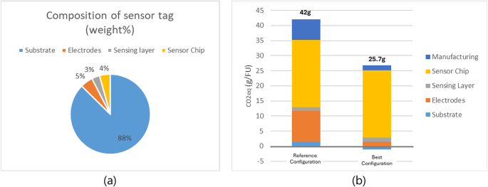
(a) Composition of the reference sensor tag in weight%; (b) Global warming potential (GWP) of the sensor tag in the reference and best configuration.
Although the substrate material accounts for around 88% of the sensor tag’s weight (Fig. 5a), it contributes only 3.2% of the environmental impact in terms of GHG emissions in the reference configuration. While this aspect could be further optimized by using bio-PE as the substrate, the substrate’s contribution to the overall environmental impact is surprisingly small. This finding contrasts with the emphasis placed on substrate materials in scientific literature, where their environmental impact often receives a disproportionate focus.
However, different configurations face technical limitations, due to the fact that not all material combinations are equally feasible. For instance, while bio-PE may optimize environmental impact, further testing is essential to ensure durability, as the actual lifespan of the substrate influences the product’s sustainability. Additionally, certain techniques, such as inkjet printing with Cu, remain technically underdeveloped. Cu inks often require thermal curing, which is incompatible with temperature-sensitive substrates like PLA and bio-PE. Furthermore, Cu ink tends to be brittle and is prone to cracking during curing, most probably due to large differences in the thermal expansion coefficients of the electrodes and the substrate. Figure 6 shows an example of Cu electrodes fabricated by means of screen printing and cured with IPL on bio-PE substrate, which exhibits cracks in the printed traces with consequent interruption of the electrical connection. This highlights the ongoing challenges and emphasizes the need for further research and development to improve the mechanical stability and performance of such material combinations in printed electronics.
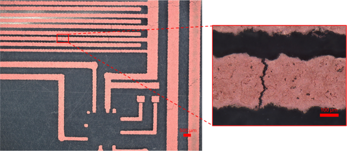
Optical microscopy image of copper nanoparticle electrodes screen printed on transparent bio-PE foil after curing with intense pulse light; The magnified image shows cracks disrupting the printed lines.
The results of the individual LCA stages are discussed in more detail in the following sections.
-
A.
Raw materials
Figure 7a and Table 7 summarize the environmental impact of all materials used in the raw materials stage. It clearly shows that the impact of the substrates is low compared to the Ag NP ink, ZnO and the sensor chip. Furthermore, bioplastics hold an environmental advantage in terms of GWP as they account for the carbon absorbed during plant growth, which is subtracted from the raw materials extraction stage, as indicated in Fig. 7b. On the other hand, the production of bioplastics still relies on fossil fuels for energy during the manufacturing process. This dependency requires reduction in the future by transitioning to renewable energy sources25. When considering the LCA of polymers, it becomes clear that global warming contribution alone is not a sufficiently representative indicator of the environmental impact of plastics. For instance, biopolymers significantly contribute to acidification and eutrophication due to the use of fertilizers, pesticides, and insecticides during the cultivation phase15.
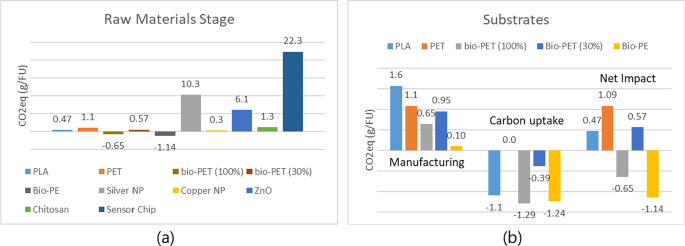
(a) Comparison of GHG emissions of all raw materials used in the fabrication of the sensor tag assuming an electrode layer thickness of 2 μm (inkjet or Aerosol Jet printing); (b) Overview of GHG emissions attributed to the substrate materials – the carbon uptake corresponds to the CO2 which is stored in bio-based polymers as it was absorbed by plants during growth.
The GWP of the Ag NP ink is much higher than that of the Cu NP ink, as shown in Fig. 7a. When screen printing with Ag NPs at a layer thickness five times greater (~ 10 μm), the CO₂ equivalent rises to over 50 g per FU, which is double the amount produced by the sensor chip. For the sensing layer, Chitosan appears to be a more environmentally sustainable choice than ZnO. Furthermore, Fig. 7a shows that the silicon chip can clearly be identified as the environmental hotspot in this stage.
-
B.
Manufacturing
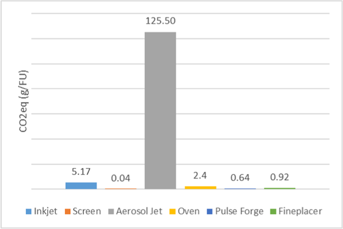
Figure 8: Global warming potential of the different manufacturing processes.
shows a comparison of the GWP of different processing technologies. Excluding the impact of cleanroom infrastructure, Aerosol Jet printing stands out due to its slow processing speed (single nozzle) and comparatively high power consumption of 2Â kW. Screen printing, while having the lowest GWP, consumes significantly more ink, which is a crucial consideration when using scarce raw materials. The assessed environmental impact of using Aerosol Jet printing for sensor tag manufacturing highlights the need to avoid over-engineering and unnecessary over-specification of requirements. For large-area electronics that do not demand high resolution or fine line widths, selecting more suitable manufacturing methods is essential to minimize not only the equipment costs, but also the environmental impact.
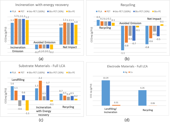
(a) Impact of the incineration with energy recovery of the different substrate materials; (b) impact of recycling of the different substrate materials; (c) result of the full LCA including raw materials stage and EoL of the substrate material; (d) result of the full LCA including raw materials stage and EoL of the electrode material.
The results of the Life Cycle Assessment (LCA) are significantly influenced by local circumstances, including the energy mix, waste management infrastructure, and availability of raw materials. Although research and development of the sensor tag are being conducted in Austria and Switzerland, these locations, as well as Europe in general, may not be the most representative for electronics manufacturing, given that the major players are based in Asia. In 2023, China had an electronics market share of 33%, followed by Taiwan with 12% and South Korea with 8%67. At the same time, China’s carbon intensity of electricity generation – measured as CO2 emissions per kWh – is over five times greater than that of Austria68. Despite a reduction in emission intensity over the past two decades, China still ranks as the fourth highest globally. This high carbon intensity is primarily due to the country’s reliance on coal power generation.
Europe’s transition to a more sustainable energy mix creates a significant business opportunity to revive electronics manufacturing in the region, particularly in contrast to cheaper production nations reliant on fossil fuels. By capitalizing on lower carbon footprints and embracing eco-friendly production practices, European manufacturers can appeal to environmentally conscious consumers as well as to global brands trying to decarbonize their supply chains.
-
C.
End of life
Global warming potential of the different manufacturing processes.
Landfilling
Substrate material: In Landfilling, only the biodegradable substrates contribute to the GWP at the EoL. Consequently, 1.1 g of CO2eq is added to the total balance of PLA (net impact as illustrated in Fig. 7b in the landfilling scenario in Fig. 9c. In general, PLA products are most often disposed of in landfills or sent to composting facilities25. However, numerous studies have indicated that PLA can be just as challenging to degrade as petroleum-based plastics without suitable conditions like elevated temperatures and adequate moisture11. According to Shruti et al.69, the most favorable environment for the biodegradation of bioplastics is composting, the worst option is landfilling. However, when discarded in natural environments like seawater and soil, their degradation is slow and might be incomplete. Consequently, their environmental impact can be rated similar to that of traditional plastics. Furthermore, bioplastics can contribute to eutrophication if not disposed of properly70. During decomposition, nutrients like carbon, nitrogen, and phosphorus may be released, promoting the growth of algae and other aquatic plants, leading to an imbalance in the ecological equilibrium of the water body. For non-degradable polymer substrates, it is assumed that no CO2eq is released in the landfilling EoL scenario, which skews the overall environmental picture, as it does not account for the potential long-term persistence of these materials in the environment.
Electrodes: Another major concern in landfilling printed electronics is the possible release of NPs in the environment55. The issue of finding strategies for the EoL of NPs is not a new one and is not necessarily driven by the emergence of printed electronics. NPs have been employed in various consumer products, including cosmetics, toothpaste, scratch-resistant eyeglasses, home disinfectants, transparent sunscreens, stain-repellent fabrics, and ceramic coatings for solar cells71,72. Studies indicate that Ag and Cu NPs can significantly bioaccumulate in plants and animals73. While the consequences for human and environmental health are still not fully understood, research indicates that these NPs can exhibit both positive and negative toxic effects in unicellular organisms as well as in more complex multi-organ systems74. Theoretically, the final printed electronic devices should not contain free or unbound NPs as they undergo sintering during the manufacturing phase, where they are heated until they bond with each other. While it is unclear whether all the NPs are effectively sintered or how strong the resulting cohesion is, a study by Roshanghias et al.75 suggests that thermal sintering results in the highest degree of NP fusion. Furthermore, the choice of substrate material influences the release rate of NPs in the environment76. On the other hand, Lee et al.77 have demonstrated that with current standards, Ag NPs cannot penetrate landfill clay liners, and that the mobility of Ag NPs was quite low over a simulation period of 100 years. This suggests that existing landfill liner standards are effective in preventing the leakage of Ag NPs. It can be assumed that the same applies for Cu NPs. Although NPs might be safely stored in landfills, this represents a significant loss of economic value and raw materials, necessitating the production of virgin metals. In general, current metal recovery practices face significant inefficiencies, with approximately 50% of metal waste ending up in municipal waste instead of being properly collected for recycling78.
Sensing materials: Unmodified Chitosan film decomposes in soil environment within 2 weeks79. This means that during landfilling, the CO2 stored in the Chitosan film as biogenic CO2 can be considered to be fully released. The carbon content of Chitosan is approximately 39.74%80. Given the molecular weight of CO2 (44 g/mol) and the atomic mass of Carbon (12 g/mol), 1 kg of Chitosan stores about 0.4 kg of Carbon resulting in a CO2 emission of 1.47 kg per kg of Chitosan. Given small amount of Chitosan on one sensor tag this means that the disposal in landfilling adds only 0.02 g of CO2eq to the total balance (see Table 6).
In contrast, ZnO is an inorganic compound, which means it cannot undergo biodegradation, leading to other environmental implications. The ecotoxicity and environmental risks associated with ZnO, in particular ZnO NPs, are closely linked to their stability. Landfills represent complex environmental systems where various pollutants coexist. Li et al.81 examined the stability and potential ecotoxicity of ZnO NPs in the presence of different heavy metals commonly found in landfill environments. The study highlights that while some interactions may reduce the immediate ecotoxicity of ZnO NPs, the long-term implications of heavy metal interactions in landfill leachate could pose significant risks to environmental health and safety. Furthermore, research indicates that current geosynthetic clay liners in the anti-seepage systems of municipal solid waste landfills are not effective at preventing ZnO NP pollution82. Like for many NPs, there is still a lack of consent among researchers leading to uncertainty regarding their true toxicity. Considering human health, ZnO is generally approved as a safe substance to ingest by the Food and Drug Administration83. Conversely, some researchers claim that ZnO is “extremely toxic� to aquatic organisms84. However, toxicological responses may vary widely among different species, including bacteria, algae, crustaceans, and fish.
Sensor chip: Overall, while silicon chips themselves may not pose significant immediate environmental hazards if landfilled, their long-term persistence and potential for leaching highlight the importance of responsible EoL management practices, such as recycling and proper disposal.
Incineration with energy recovery
In 2023, the waste-to-energy capacity in Europe reached 5.05 GW85. However, the environmental impact of incineration with energy recovery varies significantly by geographic location. In Europe, energy production relies heavily on renewables and the CO2 emissions per kWh of energy produced are relatively low compared to global averages. Consequently, the combustion of waste does not avoid as much fossil emissions as in other regions in absolute terms. Additionally, Europe’s incineration plants typically operate with a low energy recovery efficiency of around 25%, which further diminishes the potential environmental benefits of waste incineration86.
Substrate material: The actual CO2eq values for incineration of plastics, such as PET, are unknown due to the significant influence of incineration temperature on the chemical composition of the gas products60,87. Additionally, variations in combustion efficiency and operational conditions further complicate accurate emissions estimations. Another factor limiting the accuracy of the quantitative assessment is the uncertainty of the true NCV. While the best method is to determine the NCV experimentally, this data is often specific to particular conditions and may not be available for all materials. In such cases, Eq. (3) can be used to estimate the NCV, though it has limitations such as not accounting for impurities, moisture content, and incomplete combustion. Keeping those limitations in mind, the LCA revealed an avoided emission of around 0.2 g of CO2eq when incinerating a single sensor tag, more or less independent of the type of polymer substrate, as illustrated in Fig. 9a. This results in a net impact of incineration in the range of 0.9 –1.1 g.
Electrode material: When metal waste enters incineration facilities, it either melts or remains largely unaffected, depending on its melting point and the incineration temperature, but in either case, it does not contribute to energy generation. The remnants are incorporated into the bottom ash. When incinerating one ton of municipal solid waste, roughly 250 kg of bottom ash is produced, of which 10–12% are metals88. For perspective, per year 3.3 t of Ag NPs land in incineration facilities in Switzerland alone89 which has an approximate worth of 2.8 million Euros. According to a study by Mueller et al.90, approximately 58% of the Ag NPs entering the incineration process will end up in the bottom ash. However, economic recovery methods are currently limited to native metal pieces larger than 0.3 mm91. Ag-based electrodes will melt during incineration (the melting point of Ag is 960 °C), hence they are likely to form larger compounds. It is expected, however, that the resulting pieces will be smaller than the 0.3 mm recovery threshold. This suggests that there are currently no practical methods available for recovering metals from electrodes used in printed electronics from incineration ash. Most of the residual bottom ash is typically landfilled, however, there are endeavors to utilize the bottom ash in the construction industry, e.g. as a replacement for sand in concrete and for road constructions92. Regardless, the electrode material ends up either in the environment or confined to landfills. Since the electrode material is no longer in NP form after incineration the eco-toxic risk is reduced, nonetheless its economic value is lost.
Sensing material: Due to the absence of experimental data, the NCV of Chitosan was calculated according to Eq. (4) and equals 14 MJ/kg, which is relatively low compared to other polymers. In reality, the NCV might be even lower due to the hydrophilic nature and thus higher humidity content of Chitosan. Research even reports the successful use of Chitosan as flame retardant93, indicating that its efficiency for incineration with energy recovery might be even lower than assumed in this study. However, the calculated avoided emissions from the Chitosan layer when incinerating one sensor tag amount to only 4 mg of CO2eq, which is negligible.
ZnO as inorganic material is not combustible and relatively stable under high temperatures. In the United States, an estimated 38.8 t of ZnO are processed in incineration facilities annually89. It is assumed that the majority (62%) of ZnO ends up in bottom ash, with only 3% in fly ash90. Similar to the electrode material, this means that after incineration the ZnO ultimately either ends up either in landfill or somewhere in the environment, as bottom ash is commonly repurposed in the construction industry.
Recycling
In the context of emerging technologies like printed electronics, the development and implementation of sustainable practices present a classic “chicken-and-egg� dilemma. On the one hand, designing products to be recyclable may seem impractical if the necessary recycling processes are not yet in place. On the other hand, the demand for these processes will only arise if recyclable products become more prevalent. A recent review of Design for Recycling methods and guidelines highlighted significant gaps in the field, revealing that many existing approaches lack validation through recycling tests or real-world application by design practitioners94.
Substrate: The avoided emissions of recycled polymers are significant compared to the emissions associated with the recycling process itself, leading to a net negative impact for nearly all substrate materials considered, as shown in Fig. 9b. However, the actual recycling yield is mainly dependent on the degree of contamination, as well as challenges in separation of the materials. PET is generally expected to have a high process yield due to well-established collection and sorting systems. Similarly, bio-PE can be effectively recycled, although its recycling infrastructure is not as advanced as that of PET95. For PLA, a lower yield can be assumed compared to PET, due to the challenges in separating PLA from other plastics and degradation during the recycling process. While under laboratory condition high recycling yields of up to 96% can be achieved96, in practice the recycling of PLA is uneconomic at present and still results in poor-quality recycled products97. For example, Agbakoba et al.98 reported that 3D-printed structures made from 50% waste PLA exhibited a 29% decrease in tensile strength.
Electrode material: Unlike plastics, metals like Ag and Cu can theoretically be recycled indefinitely without the loss of quality. However, when it comes to electrode material in printed electronics applications, the metal cannot be recovered in its NP form, as the NPs are sintered during fabrication. Consequently, recycling in this context refers to the recycling of bulk material. It is generally accepted that recycling metals results in an 80% reduction in CO2 emissions compared to the use of virgin materials99. However, despite using recycled metal, the GWP of Ag NPs remains 100 times higher than that of Cu NPs, as indicated in Fig. 9d.
Sensing material: Chitosan, as a raw material, is commonly considered as a “recycledâ€� product since it is typically derived from waste generated in the seafood industry. Additionally, researchers are exploring alternative sources, such as extracting Chitosan from plant waste100. However, despite the use of the term “recyclingâ€� in these contexts, it does not represent recycling in the true sense of closing the material loop. Currently, there are no established processes for the actual recycling of Chitosan from waste, making it impossible to estimate the potential environmental impact or the avoided emissions associated with Chitosan recycling at present. One reason for this, as already discussed back in 1995 by Martin G. Peter101, might be that there is little economic value added and potentially no ecological benefit from recycling, since Chitosan is derived from waste materials that can easily cover global demand at present. However, while the Chitosan market is expected to continuously grow102, the availability of its primary raw material – fishery byproducts – is facing challenges. Fish production in the capture sector has declined due to factors such as overfishing, the capture of endangered species, pollution, and other environmental pressures, with climate change being the most significant contributor103. These opposing developments could make recycled Chitosan a necessary and economically viable material source in the future.
Similarly, there is no established recycling process for ZnO NPs, despite their widespread use in products such as cosmetics, batteries, and coatings. However, developing recycling strategies for ZnO from different waste sources is an area of active research104,105,106.
Sensor chip: Silicon recycling is feasible in principle, as demonstrated in the photovoltaics industry107,108. Traditional solar panels use large amounts of silicon that are generally free of complex structures and contaminants, allowing for high-purity silicon recovery. In contrast to that, recycling integrated circuits is particularly complex due to their highly integrated, multi-layered structures109. Composed of various materials, from plastics to metal alloys, and containing hazardous chemicals, each semiconductor component has unique recycling requirements. Current methods largely emphasize recovering high-value metals like gold and Ag, however, there is no established process for recycling silicon chips. At present, there is no reliable LCA data for silicon chip recycling available110.
Conclusion and recommendations
Printed hybrid sensors, as published before20, offer both opportunities and challenges in the context of environmental sustainability. On the opportunity side, they provide material and energy efficiency, utilize eventually eco-friendly material options such as bio-based and biodegradable substrates, and clearly have the potential to minimize carbon emissions, particularly in single-use applications. However, challenges persist, notably in recycling and EoL management due to high integration levels and potential risks from NPs. Achieving reliable functionality in these sensor systems still relies heavily on silicon chips, which represent a significant environmental hotspot, particularly if disposed of while still functioning, as discussed in this study. A similar issue exists in retail, where RFID tags, commonly embedded in packaging, are disposed of after single use, exacerbating waste concerns and highlighting the growing prevalence of short-lived electronic components111. In this sense, the present study is a representative analysis of the environmental impacts associated with disposable sensor technology. Ultimately, the eco-friendliness of printed hybrid sensors depends on the specific use case and context.
While sustainability in product development is often seen as a burden and driven by legal requirements, it also presents economic opportunities. By reducing the amount of material or energy used in a process, costs are lowered, leading to more efficient and competitive products. Additionally, incorporating recycled materials further cut costs and create value by relying on more sustainable supply chains, while attracting environmentally conscious customers.
It is essential for vendors and manufacturers to take responsibility for the EoL management of their products already at the design and development phase following principles like “design for recycling�. Even for mass products, such as silicon chips, reliable data on the assessment of the environmental impact of different EoL options is still scarce110. In contrast, the polymer industry is significantly more advanced in providing LCA data. Implementing a collection system, such as a deposit-return scheme, can facilitate the recycling process and ensure proper disposal, similar to initiatives seen with consumables such as coffee capsules112 and heated tobacco products113. By establishing strong re-collection infrastructure and optimizing recycling processes tailored to the specific materials of their products, manufacturers will also secure a more sustainable flow of raw materials, reducing the need for virgin resources while contributing to a circular economy.
When establishing a recycling process, emphasis is given to the most valuable components to recover. This is not limited to the economic value, but also includes the criticality of the raw materials. In printed electronics with Ag conductive traces, this means prioritizing the recycling of the electrode material, as it carries a much higher environmental burden than the polymer substrate. However, when Cu is used instead, the LCA suggests that focusing on recycling the substrate would be a more responsible choice.
The results of this LCA indicate that the environmental impact of the printed components of the sensor tag can be reduced by 39% through optimizing the configuration, while the silicon chip remains an environmental hotspot. This insight demands re-thinking the design of the device. As an example, a strategy of integrating the sensor chip into a reusable device, such as a phone case, would be a more sustainable design choice as it drastically prolongs the use phase of the silicon chip. The printed sensor patch, adhesively attached to the case, would be the only component requiring disposal and replacement after its functional lifespan. Another approach is to design the sensor in a way that the chip can be easily separated from the printed part for reuse or recycling. While current innovations focus on dissolving substrates to recover silicon electronics114,115, strategies for recovering both the substrate and the chip are still lacking.
Overall, LCA has proven to be an invaluable tool for informing decision-making in the design of hybrid electronic sensor systems, though a significant gap in research regarding EoL processes and the associated impacts has become apparent. This lack of data and absence of established methods for EoL management creates uncertainty, particularly in assessing the environmental impact and recyclability of hybrid electronic sensor systems.
Data availability
The data is presented in the manuscript, further detailed data can be obtained from the corresponding author upon request.
References
-
Ongaro, A. E. et al. Engineering a sustainable future for point-of-care diagnostics and single-use microfluidic devices. Lab. Chip. Bd. 22, 3122–3137 (2022).
-
Misra, N. R., Kumar, S. & Jain, A. A Review on E-waste: Fostering the Need for green electronics. In International Conference on Computing, Communication, and Intelligent Systems (ICCCIS), Greater Noida, India, 2021., Greater Noida, India, 2021. (2021).
-
UNITAR & THE GLOBAL E-WASTE MONITOR 2024. (2024).
-
Greenly, C. et al. Observing and tracking the great pacific garbage patch, in Small Satellite Conference, (2021).
-
Kuper, J. & Hojsik, M. Poisoning the poor – electronic waste in Ghana. (2008). https://wayback.archive-it.org/9650/20200513123835/http://p3-raw.greenpeace.org/international/Global/international/planet-2/report/2008/9/poisoning-the-poor-electonic.pdf. [Zugriff am 18 November 2024].
-
Merino-Jimenez, I. et al. Sabaté, A Self-Powered minimalistic glucometer: A lean approach to sustainable single-use point-of-care devices. Adv. Mater. Technol. Bd. 6(Nr. 5), 2001051 (2021).
-
Costa, M. N. et al. A low cost, safe, disposable, rapid and self-sustainable paper-based platform for diagnostic testing: Lab-on-paper. Nanotechnol. Bd 25(Nr. 9), 094006 (2014).
-
Batet, D., Vilaseca, F., Eloi, R. & Esquivel, J. P. Gabriel, Experimental overview for green printed electronics: Inks, substrates, and printing techniques. Flex. Print. Electron. Bd. 8(Nr. 2), 024001 (2023).
-
Hussein, R. N., Schlingman, K., Noade, C., Carmichael, R. S. & Carmichael, T. B. Shellac-paper composite as a green substrate for printed electronics. Flex. Print. Electron. Bd. 7(Nr. 4), 045007 (2022).
-
Luoma, E., Välimäki, M., Ollila, J., Heikkinen, K. & Immonen, K. Bio-based polymeric substrates for printed hybrid electronics. Polymers, Bd. 14, Nr. 9, 1863 (2022).
-
Nandakumar, A., Chuah, J. A. & Sudesh, K. Bioplastics: A boon or bane?? Renew. Sustain. Energy Rev. Bd. 147, 111237 (2021).
-
Harrison, J. P., Boardman, C., O’Callaghan, K., Delort, A. M. & Song, J. Biodegradability standards for carrier bags and plastic films in aquatic environments: A critical review. R. Soc. Open. Sci., Bd.5, Nr. 5, (2018).
-
Campanale, C. et al. A critical review of biodegradable plastic mulch films in agriculture: Definitions, scientific background and potential impacts. Trends Anal. Chem. Bd. 170, 117391 (2024).
-
Zhu, J. & Wang, C. Biodegradable plastics: Green hope or greenwashing? Marine Pollut. Bull. Bd. 161, Nr. B, 111774 (2020).
-
Albrecht, K. et al. Thema: Integration Von Ökologischen Kennwerten Biobasierter Werkstoffe in Den Industriellen Planungs- Und Konstruktionsprozess – Methodologie Und Werkzeuge: Schlussbericht Zum Verbundvorhaben: Gemeinsamer Bericht Aller Partner : Laufzeit: 01.07.2017 Bis (Ford Werke GmbH, 2020).
-
Chandrasekaran, S., Jayakumar, A. & Velu, R. A comprehensive review on printed electronics: A technology drift towards a sustainable future. Nanomaterials Bd. 12(Nr. 23), 4251 (2022).
-
Rebitzer, G. et al. und D. W. Pennington, life cycle assessment: Part 1: Framework, goal and scope definition, inventory analysis, and applications, Environment Int. Bd. 30(Nr. 5), 701–720 (2004).
-
Bjørn, A., Owsianiak, M. & Molin, C. und M. Z. Hauschild, LCA history, in life cycle assessment 17–30 (Springer, 2017).
-
EPA – United States Environmental Protection Agency. Understanding Global Warming Potentials, 8 August 2024. [Online]. https://www.epa.gov/ghgemissions/understanding-global-warming-potentials. [Zugriff am 18 November 2024].
-
Zikulnig, J. et al. Eco-conscious approach to wireless gas monitoring with a hybrid printed passive sensor Tag. IEEE Sens. Lett. Bd. 8(Nr. 6), 5501904 (2024).
-
Technical Committee, I. S. O. T. C. & 207 ISO 14040:2006(en) Environmental management—life cycle assessment—principles and framework (International Organization of Standardization (ISO), 2006).
-
Wiklund, J. et al. A review on printed electronics: Fabrication methods, inks, substrates, applications and environmental impacts. J. Manuf. Mater. Process. Bd. 5(Nr. 3), 89 (2021).
-
Tan, H. W., Choong, Y. Y. C., Kuo, C. N., Low, H. Y. & Chua, C. K. 3D printed electronics: Processes, materials and future trends. Prog. Mater. Sci. Bd. 127, 100945 (2022).
-
Mirkhalaf, S. M. & Fagerström, M. The mechanical behavior of polylactic acid (PLA) films: Fabrication, experiments and modelling. Mechanics Time-Dependent Mater. Bd. 25, 119–131 (2019).
-
Ghomi, E. R. et al. The life cycle assessment for polylactic acid (PLA) to make it a low-carbon material. Polymers Bd. 13(Nr. 11), 1854 (2021).
-
Ali, S. S. et al. Sun, bioplastic production in terms of life cycle assessment: A state-of-the-art review. Environ. Sci. Ecotechnol. Bd. 15, 100254 (2023).
-
Volanti, M. et al. Terephthalic acid from renewable sources: Early-stage sustainability analysis of a bio-PET precursor. Green Chem. Nr. 4, (2019).
-
The CocaCola Company. CocaCola Collaborates with Tech Partners to Create Bottle Prototype Made from 100% Plant-Based Sources, 22 October 2021. [Online]. https://www.coca-colacompany.com/media-center/100-percent-plant-based-plastic-bottle. [Zugriff am 19 August 2024].
-
CSR Activity Report (CSR Guideline Activity Reports. ) – Contributing Solutions to Social Issues through Business Activities – Realizing a Circular Economy, TORAY INDUSTRIES, INC., 2024. [Online]. https://www.toray.com/global/sustainability/activity/social/recycling.html. [Zugriff am 19 August 2024].
-
Dimitriou, E. & Michailidis, N. Printable conductive inks used for the fabrication of electronics: An overview, Nanotechnology Bd. 32, 502009 (2021).
-
Slotte, M. & Zevenhoven, R. Energy requirements and life cycle assessment of production and product integration of silver, copper and zinc nanoparticles. J. Clean. Prod. Bd. 148, 948–957 (2017).
-
Taleat, Z., Khoshroo, A. & Mazloum-Ardakani, M. Screen-printed electrodes for biosensing: A review (2008–2013), Microchimica Acta Bd. 181, 865–891 (2014).
-
Tulliani, J. M., Inserra, B. & Ziegler, D. Carbon-based materials for humidity sensing: A short review. Micromachines Bd. 10(Nr. 4), 232 (2019).
-
Hosseini, E. S., Dervin, S., Ganguly, P. & Dahiya, R. Biodegradable materials for sustainable health monitoring devices. ACS Appl. Bio Mater. Bd. 4(Nr. 1), 163–194 (2020).
-
Sui, Y. et al. Whiting, A reactive inkjet printing process for fabricating biodegradable conductive zinc structures. Adv. Eng. Mater. Bd. 25(Nr. 1), 2200529 (2022).
-
Baumbauer, C. L., Gopalakrishnan, A., Atreya, M., Whiting, G. L. & Arias, A. C. Polycaprolactone-Based zinc ink for high conductivity transient printed electronics and antennas. Adv. Electron. Mater. Bd. 10(Nr. 4), 2300658 (2024).
-
Kou, S. G., Peters, L. M. & Mucalo, M. R. Chitosan: A review of sources and preparation methods. Int. J. Biol. Macromol. Bd. 169, 85–94 (2021).
-
Elsabee, M. Z. & Abdou, E. S. Chitosan based edible films and coatings: A review. Mater. Sci. Eng. C. Bd. 33(Nr. 4), 1819–1841 (2013).
-
Zangmeister, R. A., Park, J. J., Rubloff, G. W. & Tarlov, M. J. Electrochemical study of Chitosan films deposited from solution at reducing potentials. Electrochim. Acta. Bd. 51, 5324–5333 (2006).
-
Nasution, T. I., Nainggolan, I., Hutagalung, S. D., Ahmad, K. R. & Ahmad, Z. A. The sensing mechanism and detection of low concentration acetone using chitosan-based sensors. Sens. Actuators B. Bd. 177, 522–528 (2013).
-
Sadeghian Lemraski, M. & Nadimi, E. Acetone gas sensing mechanism on zinc oxide surfaces: A first principles calculation. Surf. Sci. Bd. 657, 96–103 (2017).
-
Zhu, L. & Zeng, W. Room-temperature gas sensing of ZnO-based gas sensor: A review. Sens. Actuators A Phys. Bd. 267, 242–261 (2017).
-
Pawlik, V. Höhe der CO₂-Emissionen durch Stromerzeugung in der EU nach Ländern im Jahr 2022, Statista.com, 5 July 2024. [Online]. https://de.statista.com/statistik/daten/studie/1009521/umfrage/co2-emissionen-durch-stromerzeugung-in-der-eu/. [Zugriff am 17 July 2024].
-
THE EUROPEAN PARLIAMENT AND THE COUNCIL OF THE EUROPEAN & UNION Directive 2008/98/EC of the European Parliament and of the Council of 19 November 2008 on waste and repealing certain directives (Text with EEA relevance) (2008).
-
Otero, F. & Magner, E. Biosensors—recent advances and future challenges in electrode materials. Sensors Bd. 20(Nr. 12), 3561 (2020).
-
Eurostat, W. Statistics, January 2023. [Online]. https://ec.europa.eu/eurostat/statistics-explained/index.php?title=Waste_statistics. [Zugriff am 13 June 2024].
-
Yadav, V. et al. Framework for quantifying environmental losses of plastics from landfills. Resour. Conserv. Recycl. Bd. 161, 104014 (2020).
-
Ma, Y., He, P., Lü, F. & Zhang, H. Improving the method for calculating carbon emissions from waste incineration: Confirmed with carbon-14 testing of flue gas. Carbon Res. Bd. 3, 74 (2024).
-
Johnke, B. et al. Good Practice Guidance and Uncertainty Management in National Greenhouse Gas Inventories, pp. 455–468 (2000).
-
Hogg, D. Debunking Efficient Recovery – The Performance of EU Incineration Facilities, Zero Waste Europe (2023).
-
Hosokai, S., Matsuoka, K., Kuramoto, K. & Suzuki, Y. Modification of Dulong’s formula to estimate heating value of gas, liquid and solid fuels. Fuel Process. Technol. Bd. 152, 399–405 (2016).
-
Rossi, V. et al. Life cycle assessment of end-of-life options for two biodegradable packaging materials: Sound application of the European waste hierarchy. J. Clean. Prod. Bd. 86, 132–145 (2015).
-
Tonini, D., Garcia-Gutierrez, P. & Nessi, S. Environmental effects of plastic waste recycling. European Commission (2021).
-
Chen, T. et al. und J. Hester, Recy-ctronics: Designing fully recyclable electronics with varied form factors, arxiv preprint, Bd. (2024). arXiv:2406.09611.
-
Keskinen, M. 16 – End-of-life options for printed electronics. In Waste Electrical and Electronic Equipment (WEEE) Handbook, Woodhead Publishing Series in Electronic and Optical Materials, 352–364. (2012).
-
Plastics & Europe Recycling Technologies, [Online]. (2024). https://plasticseurope.org/sustainability/circularity/recycling/recycling-technologies/#:~:text=Mechanical%20recycling%20is%20the%20most,are%20relatively%20easy%20to%20recycle. [Zugriff am 17 July 2024].
-
Vogtländer, J. G. A practical guide to LCA for students designers and business managers: Cradle-to-grave and Cradle-to-cradle. VSSD (2012).
-
Sustainability, I. & Metrics Idemat 2024 Rev V1-2, 2024. [Online]. https://www.ecocostsvalue.com/data-tools-books/. [Zugriff am 6 November 2024].
-
Lase, I. S. et al. Material flow analysis and recycling performance of an improved mechanical recycling process for post-consumer flexible plastics. Waste Manag. Bd. 153, 249–263 (2022).
-
Sovová, K. et al. A study of thermal decomposition and combustion products of disposable polyethylene terephthalate (PET) plastic using high resolution fourier transform infrared spectroscopy, selected ion flow tube mass spectrometry and gas chromatography mass spectrometr, Mol. Phys. Bd. 106(Nr. 9–10), 1205–1214 (2008).
-
Prenzel, T. M., Gehring, F., Fuhs, F. & Albrecht, S. Influence of design properties of printed electronics on their environmental profile. Matériaux Techniques. Bd. 109, 5–6 (2021).
-
Muñoz, I., RodrÃguez, C., Gillet, D. & Moerschbacher, B. M. Life cycle assessment of Chitosan production in India and Europe. Int. J. Life Cycle Assess. Bd. 23, 1151–1160 (2018).
-
Ruberti, M. The chip manufacturing industry: Environmental impacts and eco-efficiency analysis. Sci. Total Environ. Bd. 858(Nr. 2), 159873 (2023).
-
Kanth, R. K. et al. Life cycle assessment of printed antenna: Comparative analysis and environmental impacts evaluation. In Proceedings of the IEEE International Symposium on Sustainable Systems and Technology Chicago, IL, USA (2011).
-
Tjorko, K. Life Cycle Assessment of microfluidic devices for point-of-care testing: A comparative analysis of PDMS, paper and PLA (2023).
-
Stieberova, B. et al. Application of ZnO nanoparticles in Self-Cleaning coating on a MetalPanel: An assessment of environmental benefits. ACS Sustain. Chem. Eng. Bd. 5(Nr. 3), 2493–2500 (2017).
-
Moore, B., TOP 10 ELECTRONICS MANUFACTURERS BY COUNTRY & Titoma February 2024. [Online]. (2023). https://titoma.com/blog/largest-electronics-manufacturers. [Zugriff am 23 May 2024].
-
Slotta, D. Carbon intensity of the power sector in China from 2000 to 2022, Statista, March [Online]. (2024). https://www.statista.com/statistics/1300419/power-generation-emission-intensity-china/#:~:text=The%20carbon%20intensity%20of%20electricity,gCO%E2%82%82%2FkWh)%20in%202022. [Zugriff am 23 May 2024].
-
Shruti, V. C. & Kutralam-Muniasamy, G. Bioplastics: Missing link in the era of microplastics. Sci. Total Environ. Bd. 697, 134139 (2019).
-
Chen, L., Pelton, R. E. & Smith, T. M. Comparative life cycle assessment of fossil and bio-based polyethylene terephthalate (PET) bottles. J. Clean. Prod. Bd. 137, 667–676 (2016).
-
Gupta, R. & Xie, H. Nanoparticles in daily life: Applications, toxicity and regulations. J. Environ. Pathol. Toxicol. Oncol. Bd. 37(Nr. 3), 209–230 (2018).
-
McGillicuddy, E. et al. Silver nanoparticles in the environment: Sources, detection and ecotoxicology. Sci. Total Environ. Bd. 575, 231–246 (2017).
-
Ameh, T. & Sayes, C. M. The potential exposure and hazards of copper nanoparticles: A review. Environ. Toxicol. Pharmacol. Bd. 71, 103220 (2019).
-
Rajan, R., Huo, P., Chandran, K. & Dakshinamoorthi, B. M. S.-I. Yun und B. Liu, A review on the toxicity of silver nanoparticles against different biosystems, Chemosphere, Bd. 292, 133397 (2022).
-
Roshanghias, A., Krivec, M. & Baumgart, M. Sintering strategies for inkjet printed metallic traces in 3D printed electronics. Flex. Print. Electron. Bd. 2(Nr. 4), 045002 (2017).
-
Atkinson, J., Joyce, T. & Joyce, M. Printed electronics: A landfill simulation study to assess environmental impacts, J. Solid Waste Technol. Manag. Bd. 43(Nr. 2), 145–150 (2017).
-
Lee, Y. S., Kim, Y. M. & Kim, Y. Evaluation of silver nanoparticles (AgNPs) penetration through a clay liner in landfills, J. Hazardous Mater. Bd. 404(Nr. A), 124098 (2021).
-
Bunge, R. Recovery of metals from waste incinerator bottom ash, Verband der Betreiber Schweizerischer Abfallverwertungsanlagen (VBSA), Bern, Switzerland (2016).
-
Wrońska, N., Katir, N., Nowak-Lange, M., El Kadib, A. & Lisowska, K. Biodegradable chitosan-based films as an alternative to plastic packaging. Foods Bd. 12(Nr. 18), 3519 (2023).
-
Lekene, R. B. N. et al. Mbadkam, High-quality low-cost activated Carbon/chitosan biocomposite for effective removal of nitrate ions from aqueous solution: Isotherm and kinetics studies. Biomass Convers. Refin. Bd. 14, 20855–20872 (2024).
-
Li, X., Ding, W., Tan, S. & Zeng, X. Stability of Nano-ZnO in simulated landfill leachate containing heavy metal ions. Ecotoxicol. Environ. Saf. Bd. 198, 110641 (2020).
-
Yang, P. et al. Transport behavior of nZnO in geosynthetic clay liner used in municipal solid waste landfills under temperature effect. Environ. Earth Sci. Bd. 77, 10 (2017).
-
U.S, Food & Drug Administration, PART 182—Substances generally recognized as safe; Subpart I – Nutrients. & ; Sect. 1828991 Zinc oxide, Code of Federal regulations Bd. 21(Nr. 3), 21CFR182.8991 (2024).
-
Wu, F., Harper, B. J. & Harper, S. L. Comparative dissolution, uptake, and toxicity of zinc oxide particles in individual aquatic species and mixed populations. Environ. Toxicol. Bd. 38(Nr. 3), 591–602 (2019).
-
Jaganmohan, M. Installed capacity of municipal waste energy in Europe from 2010 to 2023, by country, Statista.com, 28 May 2024. [Online]. https://www.statista.com/statistics/1122082/europe-waste-to-energy-capacity-by-country/. [Zugriff am 5 June 2024].
-
Equanimator Ltd for Zero Waste Europe. Debunking Efficient Recovery: The Performance of EU Incineration Facilities, (2023).
-
Mentes, D. et al. Combustion behaviour of plastic waste – A case study of PP, HDPE, PET, and mixed PES-EL. J. Clean. Prod. Bd. 402, 136850 (2023).
-
Verbinnen, B., Billen, P., Van Caneghem, J. & Vandecasteele, C. Recycling of MSWI bottom Ash: A review of chemical barriers, engineering applications and treatment technologies, Waste Biomass Valoriz. Bd. 8, 1453–1466 (2017).
-
Holder, A. L., Vejerano, E. P. & Zhou, X. Marr, nanomaterial disposal by incineration. Environmental Sci. Process. Impacts. Bd. 15, 1652–1664 (2013).
-
Mueller, N. C., Buha, J., Wang, J., Ulrich, A. & Nowack, B. Modeling the flows of engineered nanomaterials during waste handling. Environmental Sci. Process. Impacts. Bd. 15, 251 (2013).
-
Å yc, M. et al. Metal recovery from incineration bottom Ash: State-of-the-art and recent developments. J. Hazard. Mater. Bd. 393, 122433 (2020).
-
Abdullah, M. H., Rashid, A. S. A., Anuar, U. H. M., Marto, A. & Abuelgasim, R. Bottom ash utilization: A review on engineering applications and environmental aspects. IOP Conf. Ser. Mater. Sci. Eng. Bd. 527, 012006 (2019).
-
Malucelli, G. Flame-retardant systems based on chitosan and its derivatives: State of the art and perspectives. Molecules Bd. 25(Nr. 18), 4046 (2020).
-
van Dolderen, D. C., Aghaeian, S., Bakker, C. A. & Balkenende, R. Design for recycling of electronics: The urgent need for better methods. In 2024 Electronics Goes Green 2024+ (EGG), Berlin, Germany, (2024).
-
Rosenboom, J. G., Langer, R. & Traverso, G. Bioplastics for a circular economy. Nat. Rev. Mater. Bd. 7, 117–137 (2022).
-
Cosate de Andrade, M. F., Souza, P. M. S., Cavalett, O. & Morales, A. R. Life cycle assessment of Poly(Lactic Acid) (PLA): Comparison between chemical recycling, mechanical recycling and composting. J. Polym. Environ. Bd. 24, 372–384 (2016).
-
Castro-Aguirre, E., Iñiguez-Franco, F., Samsudin, H., Fang, X. & Auras, R. Poly(lactic acid)—mass production, processing, industrial applications, and end of life. Adv. Drug Deliv. Rev. Bd. 107, 333–366 (2016).
-
Agbakoba, V. C., Webb, N., Jegede, E., Phillips, R. & Hlangothi, S. P. und M. J. John, Mechanical recycling of waste PLA generated from 3D printing activities: Filament production and thermomechanical analysis. Macromol. Mater. Eng., early access, (2023).
-
EuRIC AISBL – Recycling. Bridging Circular Economy & Climate Policy, Metal Recycling Factsheet, [Online]. https://circulareconomy.europa.eu/platform/sites/default/files/euric_metal_recycling_factsheet.pdf. [Zugriff am 24 September 2024].
-
Wu, C. C., Lai, N., Chen, B. Y. & Hsueh, C. C. Feasibility study of Chitosan extraction from waste leaves of Luffa cylindrica for bioresource recycling. Sustain. Chem. Pharm. Bd. 30, 100864 (2022).
-
Peter, M. G. Applications and environmental aspects of Chitin and Chitosan. J. Macromol. Sci. Bd. 32(Nr. 4), 629–640 (1995).
-
Pellis, A., Guebitz, G. M. & Nyanhongo, G. S. Chitosan: Sources, processing and modification techniques, Gels Bd. 8(Nr. 7), 393 (2022).
-
Ghorai, T., Sharma, A., Jana, D. & Jana, S. Implications of climate change on fisheries and food security, Outlook of climate change and fish nutrition, pp. 75–84, (2023).
-
Ahmed, O. H., Altarawneh, M. & Al-Harahsheh, M. Jiang und B. Z. Dlugogorski, recycling of zincite (ZnO) via uptake of hydrogen halides. Phys. Chem. Chem. Phys. Bd. 20, 1221–1230 (2017).
-
Farzana, R., Rajaro, R., Behera, P. R. & Hassan, K. und V. Sahajwalla, Zinc oxide nanoparticles from Waste Zn-C battery via thermal route: Characterization and properties. Nanomaterials Bd. 8(Nr. 9), 717 (2018).
-
Abdelbasir, S. M., McCourt, K. M. & Lee, C. M. und D. C. Vanegas, Waste-derived nanoparticles: Synthesis approaches, environmental applications, and sustainability considerations. Front. Chem. Bd. 8 (2020).
-
Deng, R., Chang, N. L., Ouyang, Z. & Chong, C. M. A techno-economic review of silicon photovoltaic module recycling. Renew. Sustain. Energy Rev. Bd. 109, 532–550 (2019).
-
Huang, W. H. & Tao, M. A simple green process to recycle Si from crystalline-Si solar cells. In 2015 IEEE 42nd Photovoltaic Specialist Conference (PVSC), New Orleans, LA, USA (2015).
-
Kumar, A., Thorbole, A. & Gupta, R. K. Sustaining the future: Semiconductor materials and their recovery. Mater. Sci. Semiconduct. Process. Bd. 185, 108943 (2024).
-
Hess, J. C. Chip Production’s Ecological Footprint: Mapping Climate and Environmental Impact, interface (2024).
-
Ahamed, A. et al. Technical and environmental assessment of end-of-life scenarios for plastic packaging with electronic tags. Resour. Conserv. Recycl. Bd. 201, 107341 (2024).
-
Marinello, S., Balugani, E. & Gamberini, R. Coffee capsule impacts and recovery techniques: A literature review. Packag. Technol. Sci. Bd. 34, 11–12 (2021).
-
Philipp Morris International. Embedding convenience into our smoke-free consumable take-back program in Switzerland, 4 April 2023. [Online]. https://www.pmi.com/sustainability/case-studies-and-market-stories/convenience-in-smoke-free-consumable-take-back-program-in-switzerland. [Zugriff am 8 October 2024].
-
Guo, Y. et al. A dynamically hybrid crosslinked elastomer for room-temperature recyclable flexible electronic devices. Adv. Funct. Mater., Bd. 31, Nr. 50, pp. A Dynamically Hybrid Crosslinked Elastomer for Room-Temperature Recyclable Flexible Electronic Devices, (2021).
-
Shi, C. et al., Heterogeneous integration of rigid, soft, and liquid materials for self-healable, recyclable, and reconfigurable wearable electronics. Sci. Adv. Bd. 6(Nr. 45) (2020).
Acknowledgements
This work has been supported by Silicon Austria Labs (SAL), owned by the Republic of Austria, the Styrian Business Promotion Agency (SFG), the federal state of Carinthia, the Upper Austrian Research (UAR), and the Austrian Association for the Electric and Electronics Industry (FEEI).We acknowledge CCL Label in Völkermarkt for preparing and providing bio-PE samples used in this study.
Author information
Authors and Affiliations
Contributions
J.Z. was responsible for the conceptualization of the work, did the literature search and data analysis, interpretation and conclusion, prepared the main manuscript including the figures and tables. S.C. provided supervision, reviewed and edited the manuscript, and offered guidance throughout the project. J.K. contributed to supervision and project management, secured financing, and reviewed and edited the manuscript. All authors have read and approved the final version of the manuscript.
Corresponding author
Correspondence to
Johanna Zikulnig.
Ethics declarations
Competing interests
The authors declare no competing interests.
Additional information
Publisher’s note
Springer Nature remains neutral with regard to jurisdictional claims in published maps and institutional affiliations.
Rights and permissions
Open Access This article is licensed under a Creative Commons Attribution-NonCommercial-NoDerivatives 4.0 International License, which permits any non-commercial use, sharing, distribution and reproduction in any medium or format, as long as you give appropriate credit to the original author(s) and the source, provide a link to the Creative Commons licence, and indicate if you modified the licensed material. You do not have permission under this licence to share adapted material derived from this article or parts of it. The images or other third party material in this article are included in the article’s Creative Commons licence, unless indicated otherwise in a credit line to the material. If material is not included in the article’s Creative Commons licence and your intended use is not permitted by statutory regulation or exceeds the permitted use, you will need to obtain permission directly from the copyright holder. To view a copy of this licence, visit http://creativecommons.org/licenses/by-nc-nd/4.0/.
About this article
Cite this article
Zikulnig, J., Carrara, S. & Kosel, J. A life cycle assessment approach to minimize environmental impact for sustainable printed sensors.
Sci Rep 15, 10866 (2025). https://doi.org/10.1038/s41598-025-95682-8
-
Received: 17 December 2024
-
Accepted: 24 March 2025
-
Published: 29 March 2025
-
DOI: https://doi.org/10.1038/s41598-025-95682-8
Search
RECENT PRESS RELEASES
Related Post

